ChipApex | Global Electronic Components Supplier

SEARCH
Search Product
Search Post
— IC芯片 | 连接器 | 传感器 | 被动器件 —
Search productSearch post
— IC芯片 | 连接器 | 传感器 | 被动器件 —
Consult the customer manager about the wholesale price.
consultation hotline:86-132-6715-2157
email:[email protected]
Contact the product manager for consultation. One-stop consultation is available.
Do you want a lower wholesale price? Please send us your inquiry and we will reply immediately.
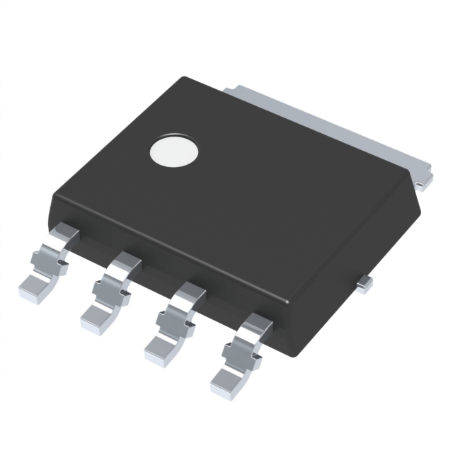
NTMYS3D8N04CLTWG is listed in the Single FETs, MOSFETs range at ChipApex. The manufacturer field lists onsemi. Its product description is MOSFET N-CH 40V 22A/87A 4LFPAK. Review the specifications below when checking this part for your BOM.
The NTMYS3D8N04CLTWG is a single N-channel power MOSFET from onsemi, utilizing Trench technology. It features a 40 V drain-to-source voltage rating and a maximum continuous drain current of 87 A at TC = 25°C. The device offers a low on-resistance of 3.7 mΩ at VGS = 10 V and 6.0 mΩ at VGS = 4.5 V. Packaged in an LFPAK4 (5x6 mm) footprint, it supports junction temperatures up to +175°C and includes a body diode with a reverse recovery time of 29 ns.
Verify the specific ordering suffix 'TWG' corresponds to the tape and reel packaging configuration containing 3000 units per reel. Confirm that the component meets RoHS compliance and lead-free manufacturing requirements as specified in the datasheet. Ensure the application environment remains within the stated thermal resistance limits for steady-state operation.
Select this component when a 40 V rating and high current capacity are required in a compact surface-mount form factor. The low gate charge characteristics make it suitable for applications requiring fast switching speeds with minimal driver stress. Evaluate thermal management needs based on the junction-to-case resistance provided in the specifications.
This part belongs to the NVMYS series of single N-channel MOSFETs designed by onsemi. It utilizes advanced trench gate technology to achieve superior performance metrics compared to standard planar devices. The LFPAK4 package is an industry-standard footprint optimized for efficient heat dissipation and board space conservation.
Direct substitutes include NVMYS3D8N04CLTWG and NVMYS3D8N04CL. Verify pinout compatibility and electrical parameters before implementation.
The maximum pulsed drain current is 520 A at TA = 25°C with a pulse width of 10 µs.
Yes, the device is AEC-Q101 qualified for automotive use.
Explore related parts through FETs, MOSFETs, Transistors, Discrete Semiconductor Products, all product categories.
 NTMYS3D8N04CLTWG

NTMYS3D8N04CLTWG is listed in the Single FETs, MOSFETs range at ChipApex. The manufacturer field lists onsemi. Its product description is MOSFET N-CH 40V 22A/87A…
Read More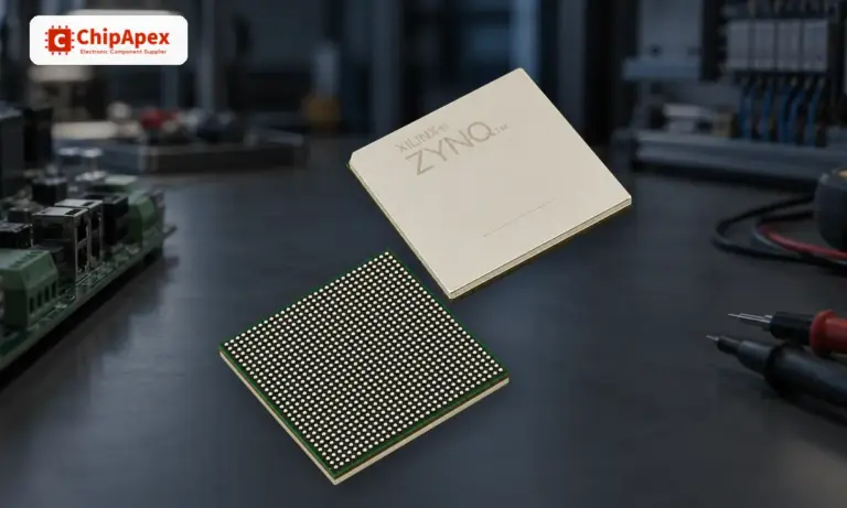
Learn what an integrated circuit is, how ICs work, the main types and the specs to check before choosing a part for your design…
Read More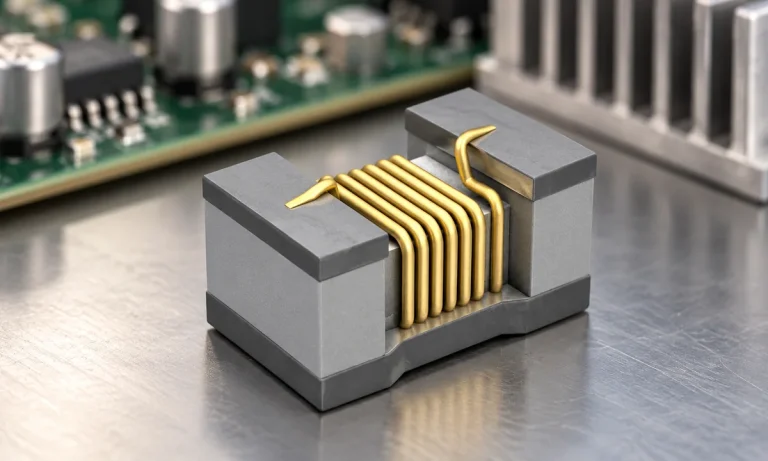
See when an inductor behaves linearly, how DC bias and saturation reduce inductance, and which current and temperature curves to check.
Read More
NTMYS3D8N04CLTWG is listed in the Single FETs, MOSFETs range at ChipApex. The manufacturer field lists onsemi. Its product description is MOSFET N-CH 40V 22A/87A…
Read More
NTMYS3D8N04CLTWG is listed in the Single FETs, MOSFETs range at ChipApex. The manufacturer field lists onsemi. Its product description is MOSFET N-CH 40V 22A/87A…
Read More
NTMYS3D8N04CLTWG is listed in the Single FETs, MOSFETs range at ChipApex. The manufacturer field lists onsemi. Its product description is MOSFET N-CH 40V 22A/87A…
Read More
NTMYS3D8N04CLTWG is listed in the Single FETs, MOSFETs range at ChipApex. The manufacturer field lists onsemi. Its product description is MOSFET N-CH 40V 22A/87A…
Read More
NTMYS3D8N04CLTWG is listed in the Single FETs, MOSFETs range at ChipApex. The manufacturer field lists onsemi. Its product description is MOSFET N-CH 40V 22A/87A…
Read More
NTMYS3D8N04CLTWG is listed in the Single FETs, MOSFETs range at ChipApex. The manufacturer field lists onsemi. Its product description is MOSFET N-CH 40V 22A/87A…
Read More
NTMYS3D8N04CLTWG is listed in the Single FETs, MOSFETs range at ChipApex. The manufacturer field lists onsemi. Its product description is MOSFET N-CH 40V 22A/87A…
Read More
NTMYS3D8N04CLTWG is listed in the Single FETs, MOSFETs range at ChipApex. The manufacturer field lists onsemi. Its product description is MOSFET N-CH 40V 22A/87A…
Read More
NTMYS3D8N04CLTWG is listed in the Single FETs, MOSFETs range at ChipApex. The manufacturer field lists onsemi. Its product description is MOSFET N-CH 40V 22A/87A…
Read More
The activity of extra discounts on wholesale prices is in full swing…
Please fill in your contact information and we will send you the latest wholesale price list.