 ChipApex | Global Electronic Components Supplier

SEARCH
Search Product
Search Post
— IC芯片 | 连接器 | 传感器 | 被动器件 —
Search productSearch post
— IC芯片 | 连接器 | 传感器 | 被动器件 —
Consult the customer manager about the wholesale price.
consultation hotline:86-132-6715-2157
email:[email protected]
Contact the product manager for consultation. One-stop consultation is available.
Do you want a lower wholesale price? Please send us your inquiry and we will reply immediately.
PCKEP14PW,118 is listed in the Clock Buffers, Drivers range at ChipApex. The manufacturer field lists NXP USA Inc.. Its product description is IC CLK BUFFER 2:5 2GHZ 20TSSOP. Review the specifications below when checking this part for your BOM.
The PCKEP14PW,118 is a low skew 1-to-5 differential clock driver manufactured by NXP USA Inc. in a TSSOP20 package. It accepts two clock sources via an input multiplexer and supports ECL, PECL, HSTL, and LVDS input signals. The device operates in PECL/HSTL mode with VCC = 2.375 V to 3.8 V (VEE = 0 V) or NECL mode with VCC = 0 V (VEE = −2.375 V to −3.8 V). Key electrical parameters include a maximum toggle frequency exceeding 2 GHz, typical propagation delay of 400 ps, within-device skew of 25 ps, and part-to-part skew of 100 ps. It features synchronous enable control to prevent runt pulses.
Verify the specific ordering suffix '118' against current manufacturer documentation to confirm packaging details and availability status. Ensure that the TSSOP20 package variant matches the design footprint requirements. Confirm moisture sensitivity level and reflow soldering profile compliance before integration into production assemblies.
Select this component when differential clock distribution with minimal skew is required for 2.5 V or 3.3 V systems. The internal multiplexer allows selection between two clock inputs based on the CLK_SEL pin state. Ensure proper termination with 50 Ω resistors to VTT (VCC - 2.0 V) for all differential outputs to maintain signal integrity and skew specifications.
The PCKEP14 series includes variants such as PCKEP14D (SO20) and PCKEP14PW (TSSOP20). The PW suffix specifically denotes the plastic thin shrink small outline package with 20 leads and a body width of 4.4 mm. This family is designed for applications demanding precise timing synchronization across multiple downstream loads.
Publicly confirmed substitute part numbers are not available in the provided source material. Designers should consult official NXP/Philips Semiconductors documentation for potential cross-references or updated product recommendations.
The enable (EN) input is synchronous. Outputs are enabled or disabled in the LOW state, avoiding runt clock pulses that can occur with asynchronous control. The internal flip-flop is clocked on the falling edge of the input clock.
The device supports PECL/HSTL mode with VCC = 2.375 V to 3.8 V and VEE = 0 V, or NECL mode with VCC = 0 V and VEE = −2.375 V to −3.8 V.
If a differential output pair is unused, both outputs may be left open (unterminated) without affecting the skew specification of other active outputs.
Explore related parts through Clock/Timing, Integrated Circuits (ICs), all product categories, ChipApex homepage.
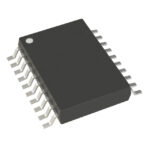 PCKEP14PW,118

Compare RC, crystal and MEMS oscillator circuits. Check ppm, jitter, load capacitance, startup margin and output compatibility before choosing a clock source.
Read More
PCKEP14PW,118 is listed in the Clock Buffers, Drivers range at ChipApex. The manufacturer field lists NXP USA Inc.. Its product description is IC CLK…
Read More
Learn what an integrated circuit is, how ICs work, the main types and the specs to check before choosing a part for your design…
Read More
PCKEP14PW,118 is listed in the Clock Buffers, Drivers range at ChipApex. The manufacturer field lists NXP USA Inc.. Its product description is IC CLK…
Read More
PCKEP14PW,118 is listed in the Clock Buffers, Drivers range at ChipApex. The manufacturer field lists NXP USA Inc.. Its product description is IC CLK…
Read More
PCKEP14PW,118 is listed in the Clock Buffers, Drivers range at ChipApex. The manufacturer field lists NXP USA Inc.. Its product description is IC CLK…
Read More
PCKEP14PW,118 is listed in the Clock Buffers, Drivers range at ChipApex. The manufacturer field lists NXP USA Inc.. Its product description is IC CLK…
Read More
PCKEP14PW,118 is listed in the Clock Buffers, Drivers range at ChipApex. The manufacturer field lists NXP USA Inc.. Its product description is IC CLK…
Read More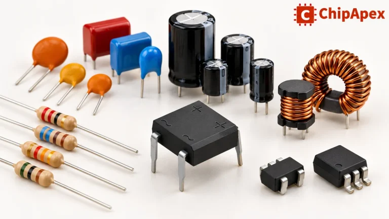
Explore electronic component types, functions, packages and datasheets. Learn selection, replacement and BOM checks before ordering parts for your PCB.
Read More
PCKEP14PW,118 is listed in the Clock Buffers, Drivers range at ChipApex. The manufacturer field lists NXP USA Inc.. Its product description is IC CLK…
Read More
Understand RF attenuator dB values, fixed and programmable types, impedance, power limits and noise tradeoffs before choosing parts for an RF signal path.
Read More
PCKEP14PW,118 is listed in the Clock Buffers, Drivers range at ChipApex. The manufacturer field lists NXP USA Inc.. Its product description is IC CLK…
Read More
The activity of extra discounts on wholesale prices is in full swing…
Please fill in your contact information and we will send you the latest wholesale price list.





