 ChipApex | Global Electronic Components Supplier

SEARCH
Search Product
Search Post
— IC芯片 | 连接器 | 传感器 | 被动器件 —
Search productSearch post
— IC芯片 | 连接器 | 传感器 | 被动器件 —
Consult the customer manager about the wholesale price.
consultation hotline:86-132-6715-2157
email:[email protected]
Contact the product manager for consultation. One-stop consultation is available.
Do you want a lower wholesale price? Please send us your inquiry and we will reply immediately.
PI6C4911505LIE is listed in the Clock Buffers, Drivers range at ChipApex. The manufacturer field lists Diodes Incorporated. Its product description is IC CLK BUFFER 2:5 1.5GHZ 20TSSOP. Review the specifications below when checking this part for your BOM.
The PI6C4911505LIE is a high-performance 1:5 LVPECL fanout buffer manufactured by Diodes Incorporated. It supports clock frequencies up to 1.5 GHz with an ultra-low additive phase jitter of typically 0.03 ps (differential, 156.25 MHz, 12 kHz to 20 MHz integration range). The device features two selectable differential inputs compatible with LVPECL, LVDS, HCSL, and CML standards. It operates on a single 3.3V power supply within the industrial temperature range of -40°C to +85°C. Packaged in a 20-pin TSSOP (L), it provides five low-skew outputs for distributing clock signals in networking and computing systems.
Verify the ordering code PI6C4911505LIEX corresponds to the specified package and suffixes. Confirm RoHS compliance and lead-free status as defined by Diodes Incorporated. Ensure the application environment stays within the -40°C to +85°C operating temperature range. Check that the input signal levels match the supported differential standards. Validate power supply stability at 3.3V ±10%.
Select this component when a 1:5 fanout ratio with LVPECL outputs is required. Ensure the system needs support for multiple differential input formats like LVDS or HCSL. Verify that the 1.5 GHz maximum frequency meets the design requirements. Consider the 20-pin TSSOP package constraints for PCB layout. Confirm that the low skew characteristics are sufficient for the target application timing budgets.
This part belongs to the PI6C4911505 series from Diodes Incorporated. It is specifically designed as a high-performance clock buffer. The 'L' indicates industrial temperature grade, and 'E' denotes lead-free packaging. It serves as a solution for distributing precise clock signals in complex digital systems.
Check for pin-compatible alternatives within the same family if different output counts are needed. Verify electrical specifications against current designs before substitution. Ensure any replacement maintains the required jitter performance and input/output voltage levels.
The maximum output frequency is 1.5 GHz.
It has two selectable differential inputs, CLK0/nCLK0 and CLK1/nCLK1, selected via the CLK_SEL pin.
The typical additive phase jitter is less than 0.03 ps, measured differentially at 156.25 MHz with a 12 kHz to 20 MHz integration range.
The device is available in a 20-pin, 173mil Wide TSSOP package.
Explore related parts through Clock/Timing, Integrated Circuits (ICs), all product categories, ChipApex homepage.
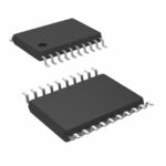 PI6C4911505LIE

PI6C4911505LIE is listed in the Clock Buffers, Drivers range at ChipApex. The manufacturer field lists Diodes Incorporated. Its product description is IC CLK BUFFER…
Read More
PI6C4911505LIE is listed in the Clock Buffers, Drivers range at ChipApex. The manufacturer field lists Diodes Incorporated. Its product description is IC CLK BUFFER…
Read More
PI6C4911505LIE is listed in the Clock Buffers, Drivers range at ChipApex. The manufacturer field lists Diodes Incorporated. Its product description is IC CLK BUFFER…
Read More
PI6C4911505LIE is listed in the Clock Buffers, Drivers range at ChipApex. The manufacturer field lists Diodes Incorporated. Its product description is IC CLK BUFFER…
Read More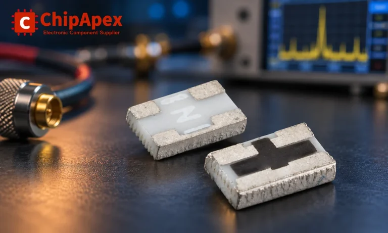
Understand RF attenuator dB values, fixed and programmable types, impedance, power limits and noise tradeoffs before choosing parts for an RF signal path.
Read More
PI6C4911505LIE is listed in the Clock Buffers, Drivers range at ChipApex. The manufacturer field lists Diodes Incorporated. Its product description is IC CLK BUFFER…
Read More
PI6C4911505LIE is listed in the Clock Buffers, Drivers range at ChipApex. The manufacturer field lists Diodes Incorporated. Its product description is IC CLK BUFFER…
Read More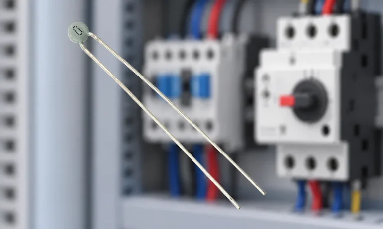
Learn why PTC resistance rises with temperature, how it differs from NTC, and which ratings matter for sensing and protection.
Read More
PI6C4911505LIE is listed in the Clock Buffers, Drivers range at ChipApex. The manufacturer field lists Diodes Incorporated. Its product description is IC CLK BUFFER…
Read More
PI6C4911505LIE is listed in the Clock Buffers, Drivers range at ChipApex. The manufacturer field lists Diodes Incorporated. Its product description is IC CLK BUFFER…
Read More
PI6C4911505LIE is listed in the Clock Buffers, Drivers range at ChipApex. The manufacturer field lists Diodes Incorporated. Its product description is IC CLK BUFFER…
Read More
PI6C4911505LIE is listed in the Clock Buffers, Drivers range at ChipApex. The manufacturer field lists Diodes Incorporated. Its product description is IC CLK BUFFER…
Read More
The activity of extra discounts on wholesale prices is in full swing…
Please fill in your contact information and we will send you the latest wholesale price list.





