 ChipApex | Global Electronic Components Supplier

SEARCH
Search Product
Search Post
— IC芯片 | 连接器 | 传感器 | 被动器件 —
Search productSearch post
— IC芯片 | 连接器 | 传感器 | 被动器件 —
Consult the customer manager about the wholesale price.
consultation hotline:86-132-6715-2157
email:[email protected]
Contact the product manager for consultation. One-stop consultation is available.
Do you want a lower wholesale price? Please send us your inquiry and we will reply immediately.
PI6CB33601ZLAIEX is listed in the Clock Buffers, Drivers range at ChipApex. The manufacturer field lists Diodes Incorporated. Its product description is IC CLK BUF 1:6 133.33MHZ 40TQFN. Review the specifications below when checking this part for your BOM.
The PI6CB33601ZLAIEX is a very low power 6-output PCIe clock buffer manufactured by Diodes Incorporated. It features an on-chip PLL and differential HCSL outputs with integrated 100Ω termination, eliminating the need for external resistors. The device supports input frequencies of 50MHz, 100MHz, 125MHz, and 133.33MHz via SMBus configuration. Operating at a nominal 3.3V supply (3.135V to 3.465V), it provides individual output enables and programmable slew rates. Packaged in a 40-lead 5x5mm TQFN, it meets PCIe Gen1 through Gen5 jitter requirements.
Verify the ZLA package suffix corresponds to the 40-contact TQFN form factor. Confirm the 'E' suffix indicates lead-free and green compliance. Ensure the 'X' suffix matches the required tape and reel orientation for automated assembly processes.
Select this component when board space is limited due to its integrated termination, which removes the requirement for 24 external resistors. Use the SMBus capability if dynamic adjustment of output slew rates or amplitudes is necessary during operation. Ensure the system requires differential HCSL signaling compatible with the specified voltage levels.
This part belongs to the PI6CB33 series of clock buffers from Diodes Incorporated. It is specifically designed as a slave-only device that utilizes a proprietary PLL architecture to achieve ultra-low jitter performance suitable for high-speed serial interfaces like PCIe.
Publicly confirmed substitute part numbers are not available in the provided documentation. Verify pinout compatibility and electrical specifications before considering alternative vendors.
The SMBus address is latched on the SADR_TRI pin upon the first assertion of the PD# signal.
The default on-chip output termination (ZOUT) is 100Ω, though it can be adjusted via SMBus registers.
Yes, the BW_SEL_TRI pin allows selection of PLL bypass mode, where the device passes the input clock directly to the outputs.
Explore related parts through Clock/Timing, Integrated Circuits (ICs), all product categories, ChipApex homepage.
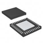 PI6CB33601ZLAIEX

PI6CB33601ZLAIEX is listed in the Clock Buffers, Drivers range at ChipApex. The manufacturer field lists Diodes Incorporated. Its product description is IC CLK BUF…
Read More
PI6CB33601ZLAIEX is listed in the Clock Buffers, Drivers range at ChipApex. The manufacturer field lists Diodes Incorporated. Its product description is IC CLK BUF…
Read More
PI6CB33601ZLAIEX is listed in the Clock Buffers, Drivers range at ChipApex. The manufacturer field lists Diodes Incorporated. Its product description is IC CLK BUF…
Read More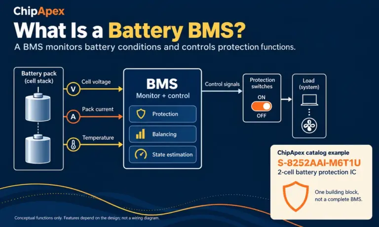
Learn what a battery BMS does, how protection differs from charging, and which pack specifications to check when sourcing BMS components through ChipApex.
Read More
PI6CB33601ZLAIEX is listed in the Clock Buffers, Drivers range at ChipApex. The manufacturer field lists Diodes Incorporated. Its product description is IC CLK BUF…
Read More
Learn why PTC resistance rises with temperature, how it differs from NTC, and which ratings matter for sensing and protection.
Read More
PI6CB33601ZLAIEX is listed in the Clock Buffers, Drivers range at ChipApex. The manufacturer field lists Diodes Incorporated. Its product description is IC CLK BUF…
Read More
PI6CB33601ZLAIEX is listed in the Clock Buffers, Drivers range at ChipApex. The manufacturer field lists Diodes Incorporated. Its product description is IC CLK BUF…
Read More
PI6CB33601ZLAIEX is listed in the Clock Buffers, Drivers range at ChipApex. The manufacturer field lists Diodes Incorporated. Its product description is IC CLK BUF…
Read More
PI6CB33601ZLAIEX is listed in the Clock Buffers, Drivers range at ChipApex. The manufacturer field lists Diodes Incorporated. Its product description is IC CLK BUF…
Read More
PI6CB33601ZLAIEX is listed in the Clock Buffers, Drivers range at ChipApex. The manufacturer field lists Diodes Incorporated. Its product description is IC CLK BUF…
Read More
PI6CB33601ZLAIEX is listed in the Clock Buffers, Drivers range at ChipApex. The manufacturer field lists Diodes Incorporated. Its product description is IC CLK BUF…
Read More
The activity of extra discounts on wholesale prices is in full swing…
Please fill in your contact information and we will send you the latest wholesale price list.






