 ChipApex | Global Electronic Components Supplier

SEARCH
Search Product
Search Post
— IC芯片 | 连接器 | 传感器 | 被动器件 —
Search productSearch post
— IC芯片 | 连接器 | 传感器 | 被动器件 —
Consult the customer manager about the wholesale price.
consultation hotline:86-132-6715-2157
email:[email protected]
Contact the product manager for consultation. One-stop consultation is available.
Do you want a lower wholesale price? Please send us your inquiry and we will reply immediately.
SCAN18540TSSC is listed in the Buffers, Drivers, Receivers, Transceivers range at ChipApex. The manufacturer field lists onsemi. Its product description is IC BUFFER INVERT 5.5V 56SSOP. Review the specifications below when checking this part for your BOM.
The SCAN18540TSSC is a high-speed, low-power inverting line driver featuring separate data inputs organized into dual 9-bit bytes with byte-oriented paired output enable control signals. This device is compliant with IEEE 1149.1 Standard Test Access Port and Boundary Scan Architecture with the incorporation of the defined boundary-scan test logic and test access port consisting of Test Data Input (TDI), Test Data Out (TDO), Test Mode Select (TMS), and Test Clock (TCK). It includes CLAMP and HIGHZ instructions and is a member of Fairchild’s SCAN products.
Verify the manufacturer origin as this component originates from Fairchild Semiconductor, which has undergone corporate restructuring. Confirm that the specific ordering code matches the required package type and ensure compatibility with existing system voltage levels and interface requirements before procurement.
Select this component for systems requiring JTAG-compliant boundary scan capabilities alongside high-speed data driving. Ensure the design accommodates the 56-Lead Shrink Small Outline Package dimensions. Verify that the operating temperature range and supply voltage specifications align with the target application environment.
The SCAN18540TSSC belongs to Fairchild’s SCAN product family, designed specifically for integrated circuit testing and data transmission. It integrates boundary-scan test logic with standard line driver functionality, allowing for both functional testing and normal data operation within a single device package.
Consult official datasheets for pin-compatible alternatives from current manufacturers following Fairchild's acquisition by onsemi. Verify electrical characteristics and package dimensions match the original specifications when considering substitutes.
The maximum TCK clock frequency is 25 MHz.
Yes, the device includes CLAMP and HIGH-Z instructions as part of its IEEE 1149.1 compliance.
There are dual output enable signals provided per byte.
Explore related parts through Logic, Integrated Circuits (ICs), all product categories, ChipApex homepage.
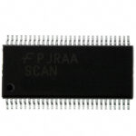 SCAN18540TSSC
SCAN18540TSSC is listed in the Buffers, Drivers, Receivers, Transceivers range at ChipApex. The manufacturer field lists onsemi. Its product description is IC BUFFER INVERT…
Read More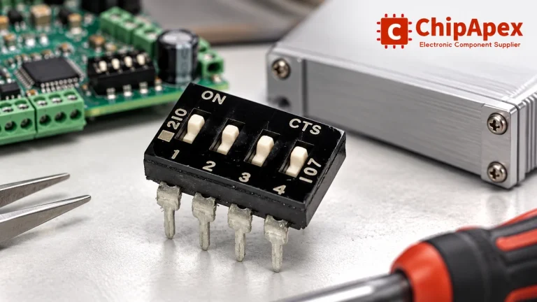
Choose a DIP switch by contact type, coded positions, footprint and signal ratings. Check logic polarity, assembly conditions and PCB configuration behavior.
Read More
SCAN18540TSSC is listed in the Buffers, Drivers, Receivers, Transceivers range at ChipApex. The manufacturer field lists onsemi. Its product description is IC BUFFER INVERT…
Read More
SCAN18540TSSC is listed in the Buffers, Drivers, Receivers, Transceivers range at ChipApex. The manufacturer field lists onsemi. Its product description is IC BUFFER INVERT…
Read More
SCAN18540TSSC is listed in the Buffers, Drivers, Receivers, Transceivers range at ChipApex. The manufacturer field lists onsemi. Its product description is IC BUFFER INVERT…
Read More
SCAN18540TSSC is listed in the Buffers, Drivers, Receivers, Transceivers range at ChipApex. The manufacturer field lists onsemi. Its product description is IC BUFFER INVERT…
Read More
SCAN18540TSSC is listed in the Buffers, Drivers, Receivers, Transceivers range at ChipApex. The manufacturer field lists onsemi. Its product description is IC BUFFER INVERT…
Read More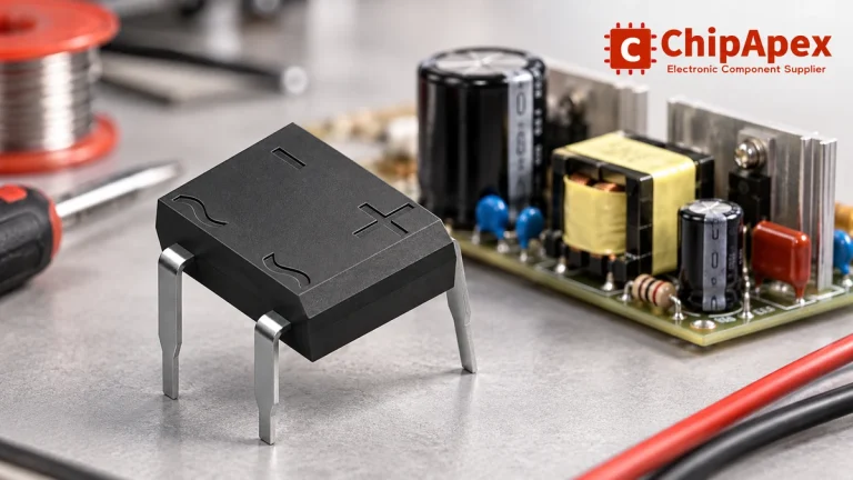
Select a bridge rectifier by reverse voltage, capacitor charging current, startup surge and cooling. Work through a stated DC voltage and ripple example.
Read More
SCAN18540TSSC is listed in the Buffers, Drivers, Receivers, Transceivers range at ChipApex. The manufacturer field lists onsemi. Its product description is IC BUFFER INVERT…
Read More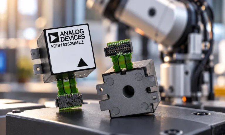
Learn what an IMU measures, how accelerometers and gyroscopes work together, why orientation estimates drift, and what to compare.
Read More
SCAN18540TSSC is listed in the Buffers, Drivers, Receivers, Transceivers range at ChipApex. The manufacturer field lists onsemi. Its product description is IC BUFFER INVERT…
Read More
Understand how a comparator switches at a voltage threshold, why hysteresis prevents chatter, and which output and input specs matter.
Read More
The activity of extra discounts on wholesale prices is in full swing…
Please fill in your contact information and we will send you the latest wholesale price list.





