 ChipApex | Global Electronic Components Supplier

SEARCH
Search Product
Search Post
— IC芯片 | 连接器 | 传感器 | 被动器件 —
Search productSearch post
— IC芯片 | 连接器 | 传感器 | 被动器件 —
Consult the customer manager about the wholesale price.
consultation hotline:86-132-6715-2157
email:[email protected]
Contact the product manager for consultation. One-stop consultation is available.
Do you want a lower wholesale price? Please send us your inquiry and we will reply immediately.
SI53302-B-GMR is listed in the Clock Buffers, Drivers range at ChipApex. The manufacturer field lists Skyworks Solutions Inc.. Its product description is IC CLK BUFFER 2:10 725MHZ 44QFN. Review the specifications below when checking this part for your BOM.
The SI53302-B-GMR is a universal fanout clock buffer featuring a 2:1 input multiplexer and ten configurable outputs. It supports any-format inputs including LVPECL, LVDS, CML, HCSL, and LVCMOS across a frequency range of 1 MHz to 725 MHz. The device delivers ultra-low additive jitter with typical performance of 50 fs rms. It incorporates built-in low-dropout regulators (LDOs) for high power supply rejection ratio (PSRR). The component operates on independent core (VDD) and output (VDDOX) supplies ranging from 1.71 V to 3.63 V. It is housed in a 44-QFN package and functions within an ambient temperature range of –40 °C to +85 °C.
Verify the 'R' suffix indicates tape and reel packaging as per the ordering guide. Confirm the specific voltage requirements for VDD and VDDOX domains match the application design. Ensure ESD precautions are taken due to moisture sensitivity classification.
Select this model when ten outputs are required alongside dual-input redundancy. Verify that the input signal formats (LVPECL, LVDS, etc.) align with the universal input termination capabilities. Check if the 1 MHz minimum frequency requirement for synchronous features meets the system's operational needs.
This part belongs to the Si5330x family of ultra-low additive jitter fanout buffers. It shares functional similarities with the Si53301 and Si53305 but offers a higher output count of ten compared to the six outputs of the Si53301.
Si53302-B-GM is the tray-packaged equivalent. Si53305-B-GM provides similar functionality with ten outputs but lacks the 2:1 input mux feature found in the Si53302.
A minimum input clock frequency of 1 MHz is required for glitchless switching and synchronous output enable features.
Unused outputs should be left unconnected to ensure proper operation.
No, LVCMOS clock input is not supported when the core supply VDD is 1.8 V; it requires 2.5 V or 3.3 V.
Explore related parts through Clock/Timing, Integrated Circuits (ICs), all product categories, ChipApex homepage.
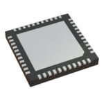 SI53302-B-GMR
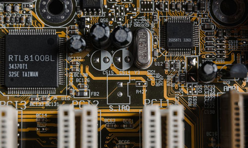
SI53302-B-GMR is listed in the Clock Buffers, Drivers range at ChipApex. The manufacturer field lists Skyworks Solutions Inc.. Its product description is IC CLK…
Read More
SI53302-B-GMR is listed in the Clock Buffers, Drivers range at ChipApex. The manufacturer field lists Skyworks Solutions Inc.. Its product description is IC CLK…
Read More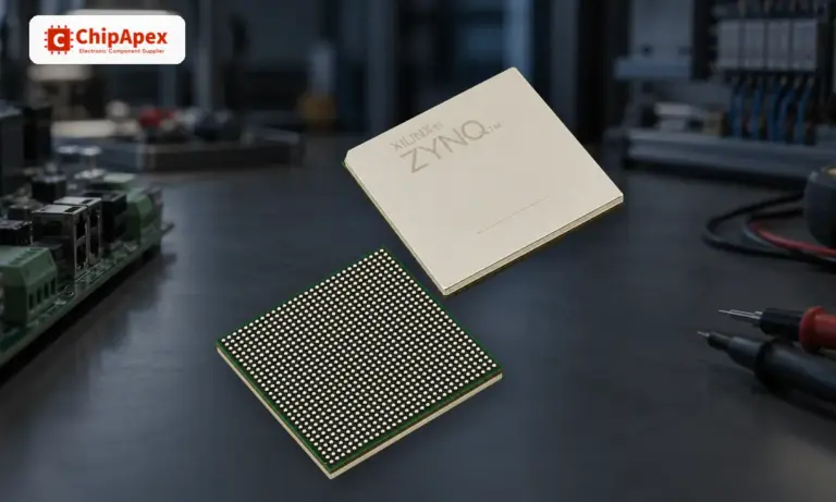
Learn what an integrated circuit is, how ICs work, the main types and the specs to check before choosing a part for your design…
Read More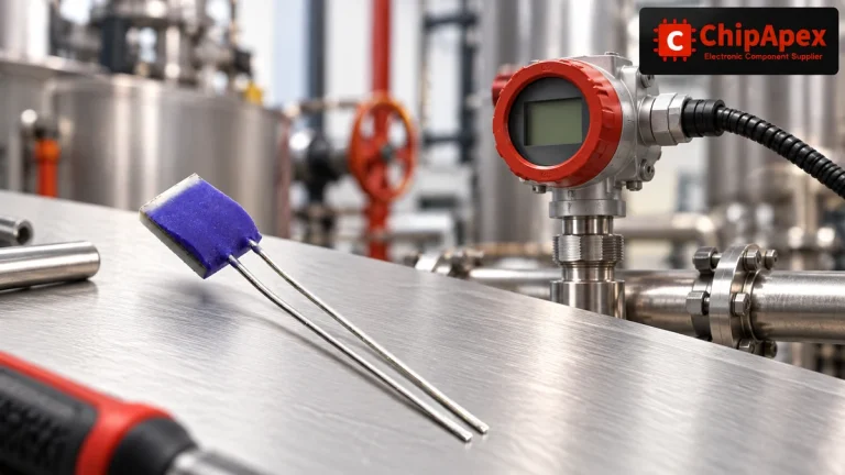
Compare Pt100 and Pt1000 RTDs, two-, three- and four-wire connections, excitation and self-heating. Build an error budget from element to reported temperature.
Read More
SI53302-B-GMR is listed in the Clock Buffers, Drivers range at ChipApex. The manufacturer field lists Skyworks Solutions Inc.. Its product description is IC CLK…
Read More
SI53302-B-GMR is listed in the Clock Buffers, Drivers range at ChipApex. The manufacturer field lists Skyworks Solutions Inc.. Its product description is IC CLK…
Read More
See how a MEMS gyroscope measures angular rate, why its angle estimate drifts, and which range, noise, interface and temperature specs to compare.
Read More
Learn what an IMU measures, how accelerometers and gyroscopes work together, why orientation estimates drift, and what to compare.
Read More
SI53302-B-GMR is listed in the Clock Buffers, Drivers range at ChipApex. The manufacturer field lists Skyworks Solutions Inc.. Its product description is IC CLK…
Read More
SI53302-B-GMR is listed in the Clock Buffers, Drivers range at ChipApex. The manufacturer field lists Skyworks Solutions Inc.. Its product description is IC CLK…
Read More
Learn how a diode conducts, how to identify anode and cathode, and when to choose rectifier, TVS, Zener or photodiode types for a circuit.
Read More
Choose a DIP switch by contact type, coded positions, footprint and signal ratings. Check logic polarity, assembly conditions and PCB configuration behavior.
Read More
The activity of extra discounts on wholesale prices is in full swing…
Please fill in your contact information and we will send you the latest wholesale price list.





