 ChipApex | Global Electronic Components Supplier

SEARCH
Search Product
Search Post
— IC芯片 | 连接器 | 传感器 | 被动器件 —
Search productSearch post
— IC芯片 | 连接器 | 传感器 | 被动器件 —
Consult the customer manager about the wholesale price.
consultation hotline:86-132-6715-2157
email:[email protected]
Contact the product manager for consultation. One-stop consultation is available.
Do you want a lower wholesale price? Please send us your inquiry and we will reply immediately.
SN74ABT543APWR is listed in the Buffers, Drivers, Receivers, Transceivers range at ChipApex. The manufacturer field lists Texas Instruments. Its product description is IC TXRX NON-INVERT 5.5V 24TSSOP. Review the specifications below when checking this part for your BOM.
The SN74ABT543APWR is an octal registered transceiver utilizing state-of-the-art EPIC-II BiCMOS design. It features two sets of D-type latches for temporary data storage and supports bidirectional data flow between A and B ports. The device provides high-drive outputs with a maximum low-level output current of 64 mA and a maximum high-level output current of -32 mA. It operates within a supply voltage range of 4.5 V to 5.5 V and is characterized for operation from -40°C to +85°C. The component is housed in a TSSOP-24 package.
Verify the specific ordering suffix 'PW' corresponds to the Thin Shrink Small-Outline (TSSOP) package configuration. Confirm that the lead finish is NIPDAU as indicated in the packaging addendum. Ensure the procurement quantity aligns with the standard large tape and reel specification of 2000 units per carrier.
Select this component when bidirectional data transfer with internal registration is required at 5V logic levels. The ABT series offers faster switching speeds compared to standard ALS or LVC families. Verify that the system power supply remains strictly within the 4.5V to 5.5V range to ensure proper functionality and avoid exceeding absolute maximum ratings.
This part belongs to the SN74ABT543A family of octal registered transceivers. It is the commercial grade version, distinct from the SN54ABT543A which is qualified for the full military temperature range. The 'PWR' suffix denotes the specific TSSOP package type and tape-and-reel shipping method.
SN74ABT543ADWR
The OE input should be tied to VCC through a pullup resistor to ensure the high-impedance state during power transitions.
CE (Chip Enable) controls data flow direction, while LE (Latch Enable) controls the transparency of the D-type latches for storing data.
Explore related parts through Logic, Integrated Circuits (ICs), all product categories, ChipApex homepage.
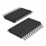 SN74ABT543APWR

SN74ABT543APWR is listed in the Buffers, Drivers, Receivers, Transceivers range at ChipApex. The manufacturer field lists Texas Instruments. Its product description is IC TXRX…
Read More
SN74ABT543APWR is listed in the Buffers, Drivers, Receivers, Transceivers range at ChipApex. The manufacturer field lists Texas Instruments. Its product description is IC TXRX…
Read More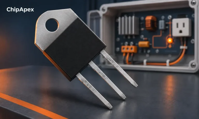
Learn how a TRIAC switches AC loads. Understand triggering, latching, holding current, phase control and thermal limits before choosing a component.
Read More
SN74ABT543APWR is listed in the Buffers, Drivers, Receivers, Transceivers range at ChipApex. The manufacturer field lists Texas Instruments. Its product description is IC TXRX…
Read More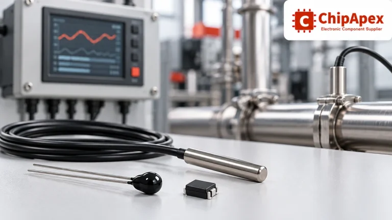
Compare thermistors, RTDs, thermocouples and temperature ICs. Learn how range, accuracy, response, interfaces and mounting affect component selection.
Read More
SN74ABT543APWR is listed in the Buffers, Drivers, Receivers, Transceivers range at ChipApex. The manufacturer field lists Texas Instruments. Its product description is IC TXRX…
Read More
SN74ABT543APWR is listed in the Buffers, Drivers, Receivers, Transceivers range at ChipApex. The manufacturer field lists Texas Instruments. Its product description is IC TXRX…
Read More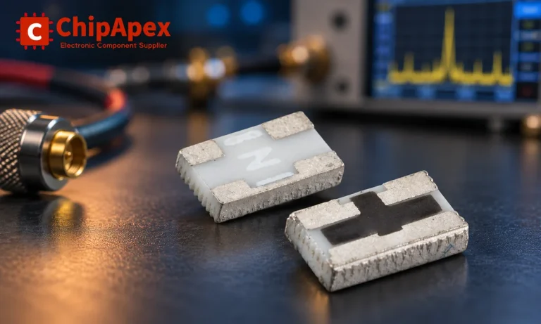
Understand RF attenuator dB values, fixed and programmable types, impedance, power limits and noise tradeoffs before choosing parts for an RF signal path.
Read More
SN74ABT543APWR is listed in the Buffers, Drivers, Receivers, Transceivers range at ChipApex. The manufacturer field lists Texas Instruments. Its product description is IC TXRX…
Read More
SN74ABT543APWR is listed in the Buffers, Drivers, Receivers, Transceivers range at ChipApex. The manufacturer field lists Texas Instruments. Its product description is IC TXRX…
Read More
SN74ABT543APWR is listed in the Buffers, Drivers, Receivers, Transceivers range at ChipApex. The manufacturer field lists Texas Instruments. Its product description is IC TXRX…
Read More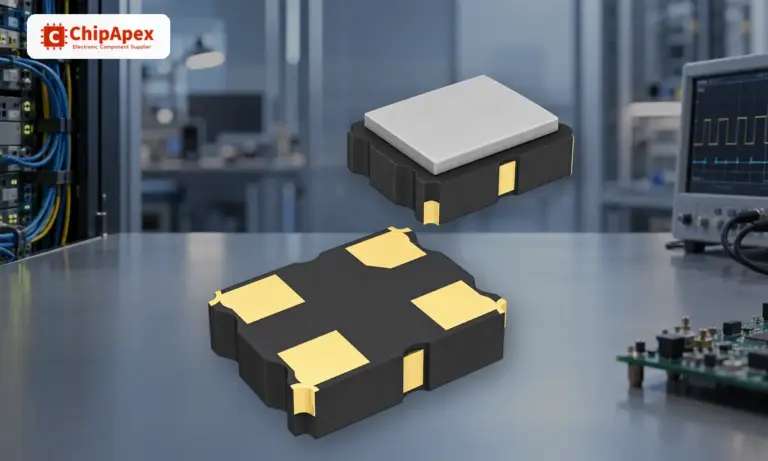
Understand how oscillators generate timing signals, how they differ from crystals, and which frequency, output and stability specs matter when choosing one.
Read More
The activity of extra discounts on wholesale prices is in full swing…
Please fill in your contact information and we will send you the latest wholesale price list.





