 ChipApex | Global Electronic Components Supplier

SEARCH
Search Product
Search Post
— IC芯片 | 连接器 | 传感器 | 被动器件 —
Search productSearch post
— IC芯片 | 连接器 | 传感器 | 被动器件 —
Consult the customer manager about the wholesale price.
consultation hotline:86-132-6715-2157
email:[email protected]
Contact the product manager for consultation. One-stop consultation is available.
Do you want a lower wholesale price? Please send us your inquiry and we will reply immediately.
SN74ACT7541QDGSRQ1 is listed in the Buffers, Drivers, Receivers, Transceivers range at ChipApex. The manufacturer field lists Texas Instruments. Its product description is AUTOMOTIVE EIGHT-CHANNEL 4.5V-TO. Review the specifications below when checking this part for your BOM.
The SN74ACT7541QDGSRQ1 is an automotive-grade octal buffer with open-drain outputs, qualified under AEC-Q100 standards. It operates within a supply voltage range of 4.5V to 5.5V and supports continuous output drive currents of 24mA at 5V, with short burst capabilities up to 75mA. The device features TTL-compatible inputs and delivers fast operation with a maximum propagation delay of 9.6ns at 5V with a 50pF load. It is housed in a 20-pin VSSOP (DGS) package.
Verify the specific ordering suffix matches the required package type, as the SN74ACT7541-Q1 family includes VQFN, TSSOP, and VSSOP options. Confirm the presence of the 'Q1' designation ensures AEC-Q100 qualification for automotive temperature grades. Check the latest Package Information Addendum for current manufacturing status and lead finish specifications before finalizing procurement.
Select this component when designing circuits requiring eight buffered channels with open-drain logic functionality in an automotive environment. Ensure the system supply voltage remains strictly between 4.5V and 5.5V to maintain specified electrical characteristics. Consider the thermal resistance metrics if operating near the upper temperature limits or driving significant capacitive loads.
This part belongs to the SN74ACT7541-Q1 family of automotive octal buffers. While other variants exist in different packages such as VQFN and TSSOP, the DGS suffix specifically denotes the VSSOP-20 package configuration. All family members share identical electrical performance and functional descriptions despite physical packaging differences.
SN74ACT7541QWRKSRQ1
Both OE1 and OE2 are active-low inputs. The outputs are enabled only when both pins are low; otherwise, all channels are forced into a high-impedance state.
Unused inputs must not be left floating. They should be terminated to either VCC or GND to prevent oscillations and excessive power consumption.
Explore related parts through Logic, Integrated Circuits (ICs), all product categories, ChipApex homepage.
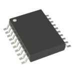 SN74ACT7541QDGSRQ1

SN74ACT7541QDGSRQ1 is listed in the Buffers, Drivers, Receivers, Transceivers range at ChipApex. The manufacturer field lists Texas Instruments. Its product description is AUTOMOTIVE EIGHT-CHANNEL…
Read More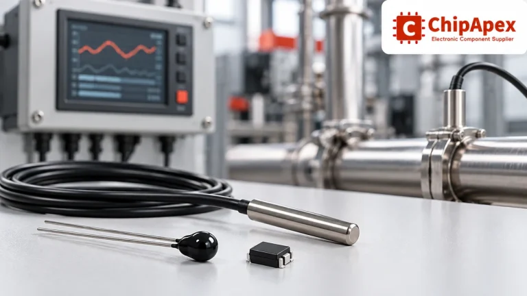
Compare thermistors, RTDs, thermocouples and temperature ICs. Learn how range, accuracy, response, interfaces and mounting affect component selection.
Read More
SN74ACT7541QDGSRQ1 is listed in the Buffers, Drivers, Receivers, Transceivers range at ChipApex. The manufacturer field lists Texas Instruments. Its product description is AUTOMOTIVE EIGHT-CHANNEL…
Read More
SN74ACT7541QDGSRQ1 is listed in the Buffers, Drivers, Receivers, Transceivers range at ChipApex. The manufacturer field lists Texas Instruments. Its product description is AUTOMOTIVE EIGHT-CHANNEL…
Read More
SN74ACT7541QDGSRQ1 is listed in the Buffers, Drivers, Receivers, Transceivers range at ChipApex. The manufacturer field lists Texas Instruments. Its product description is AUTOMOTIVE EIGHT-CHANNEL…
Read More
SN74ACT7541QDGSRQ1 is listed in the Buffers, Drivers, Receivers, Transceivers range at ChipApex. The manufacturer field lists Texas Instruments. Its product description is AUTOMOTIVE EIGHT-CHANNEL…
Read More
Select MOV varistors by continuous voltage, clamping behavior, surge waveform and repetition. Check thermal disconnection, fuse coordination and replacements.
Read More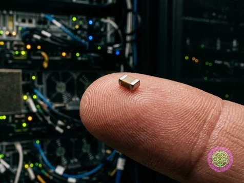
SN74ACT7541QDGSRQ1 is listed in the Buffers, Drivers, Receivers, Transceivers range at ChipApex. The manufacturer field lists Texas Instruments. Its product description is AUTOMOTIVE EIGHT-CHANNEL…
Read More
SN74ACT7541QDGSRQ1 is listed in the Buffers, Drivers, Receivers, Transceivers range at ChipApex. The manufacturer field lists Texas Instruments. Its product description is AUTOMOTIVE EIGHT-CHANNEL…
Read More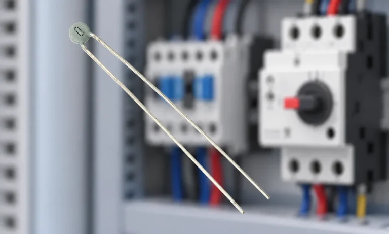
Learn why PTC resistance rises with temperature, how it differs from NTC, and which ratings matter for sensing and protection.
Read More
SN74ACT7541QDGSRQ1 is listed in the Buffers, Drivers, Receivers, Transceivers range at ChipApex. The manufacturer field lists Texas Instruments. Its product description is AUTOMOTIVE EIGHT-CHANNEL…
Read More
SN74ACT7541QDGSRQ1 is listed in the Buffers, Drivers, Receivers, Transceivers range at ChipApex. The manufacturer field lists Texas Instruments. Its product description is AUTOMOTIVE EIGHT-CHANNEL…
Read More
The activity of extra discounts on wholesale prices is in full swing…
Please fill in your contact information and we will send you the latest wholesale price list.





