 ChipApex | Global Electronic Components Supplier

SEARCH
Search Product
Search Post
— IC芯片 | 连接器 | 传感器 | 被动器件 —
Search productSearch post
— IC芯片 | 连接器 | 传感器 | 被动器件 —
Consult the customer manager about the wholesale price.
consultation hotline:86-132-6715-2157
email:[email protected]
Contact the product manager for consultation. One-stop consultation is available.
Do you want a lower wholesale price? Please send us your inquiry and we will reply immediately.
SN74ALS166DB is listed in the Shift Registers range at ChipApex. The manufacturer field lists Texas Instruments. Its product description is IC PAR-LOAD SHIFT REGIST 16-SSOP. Review the specifications below when checking this part for your BOM.
The SN74ALS166DB is a parallel-load 8-bit shift register from the Texas Instruments ALS logic family, housed in a 16-pin Shrink Small-Outline (SSOP) package. It operates within a supply voltage range of 4.5 V to 5.5 V and supports an operating temperature range of 0°C to 70°C. The device features buffered inputs with clamping diodes, synchronous loading via the SH/LD pin, and an overriding asynchronous clear (CLR). Clocking utilizes a two-input positive-NOR gate for CLK and CLK INH, enabling flexible clock control. Maximum clock frequency reaches 45 MHz, with propagation delays ranging from 2 ns to 14 ns depending on the signal path.
Verify the specific ordering suffix 'DB' corresponds to the SSOP package variant when sourcing. Confirm RoHS compliance status and lead finish details against the latest TI Package Option Addendum. Ensure the procurement channel provides valid traceability documentation for production-grade components. Cross-reference the part marking 'G166' to validate authenticity upon receipt.
Select this component for applications requiring high-speed serial shifting within standard TTL-compatible voltage levels. The ALS series offers faster switching speeds compared to standard LS logic while maintaining lower power consumption than full-speed variants. Consider the SSOP package dimensions for space-constrained printed circuit board layouts where surface-mount assembly is preferred over through-hole technology.
This device belongs to the SN74ALS166 family of parallel-load 8-bit shift registers manufactured by Texas Instruments. It is designed to be compatible with most other TTL logic families, facilitating integration into mixed-logic systems. The DB suffix specifically denotes the shrink small-outline package configuration, distinguishing it from standard SOIC or PDIP variants within the same functional family.
SN74ALS166DR
Clocking is managed through a two-input positive-NOR gate accepting CLK and CLK INH signals. Holding either input high inhibits clocking, while holding either low enables the other input, allowing the register to stop on command even if the system clock is free-running.
The SH/LD input determines the operational mode. When high, it enables serial data flow for shifting. When low, it disables serial data and enables synchronous loading of the parallel inputs (A–H) onto the flip-flops at the next clock pulse.
Explore related parts through Logic, Integrated Circuits (ICs), all product categories, ChipApex homepage.
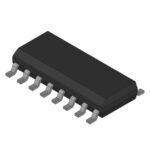 SN74ALS166DB

Choose a DIP switch by contact type, coded positions, footprint and signal ratings. Check logic polarity, assembly conditions and PCB configuration behavior.
Read More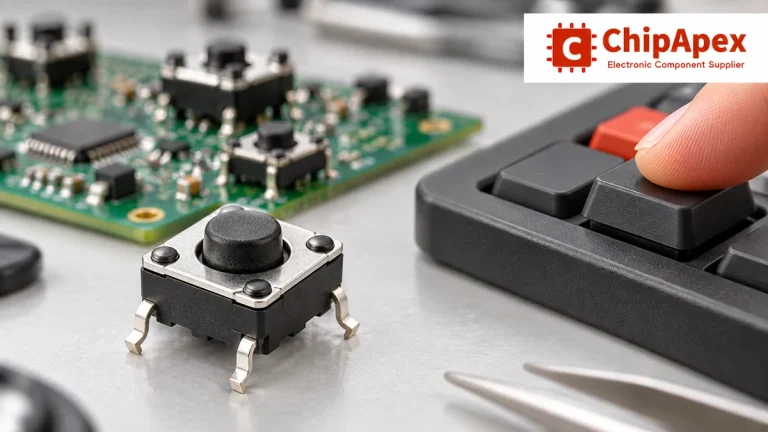
Understand tactile switches, PCB and keyboard differences, four-pin wiring, debounce, force, travel and replacement checks for reliable control inputs.
Read More
SN74ALS166DB is listed in the Shift Registers range at ChipApex. The manufacturer field lists Texas Instruments. Its product description is IC PAR-LOAD SHIFT REGIST…
Read More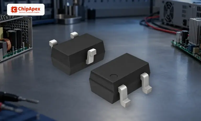
Learn how a diode conducts, how to identify anode and cathode, and when to choose rectifier, TVS, Zener or photodiode types for a circuit.
Read More
SN74ALS166DB is listed in the Shift Registers range at ChipApex. The manufacturer field lists Texas Instruments. Its product description is IC PAR-LOAD SHIFT REGIST…
Read More
SN74ALS166DB is listed in the Shift Registers range at ChipApex. The manufacturer field lists Texas Instruments. Its product description is IC PAR-LOAD SHIFT REGIST…
Read More
SN74ALS166DB is listed in the Shift Registers range at ChipApex. The manufacturer field lists Texas Instruments. Its product description is IC PAR-LOAD SHIFT REGIST…
Read More
SN74ALS166DB is listed in the Shift Registers range at ChipApex. The manufacturer field lists Texas Instruments. Its product description is IC PAR-LOAD SHIFT REGIST…
Read More
SN74ALS166DB is listed in the Shift Registers range at ChipApex. The manufacturer field lists Texas Instruments. Its product description is IC PAR-LOAD SHIFT REGIST…
Read More
SN74ALS166DB is listed in the Shift Registers range at ChipApex. The manufacturer field lists Texas Instruments. Its product description is IC PAR-LOAD SHIFT REGIST…
Read More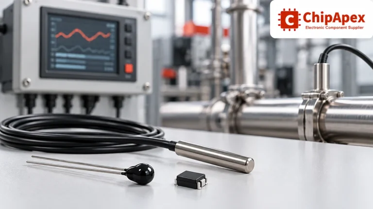
Compare thermistors, RTDs, thermocouples and temperature ICs. Learn how range, accuracy, response, interfaces and mounting affect component selection.
Read More
SN74ALS166DB is listed in the Shift Registers range at ChipApex. The manufacturer field lists Texas Instruments. Its product description is IC PAR-LOAD SHIFT REGIST…
Read More
The activity of extra discounts on wholesale prices is in full swing…
Please fill in your contact information and we will send you the latest wholesale price list.





