 ChipApex | Global Electronic Components Supplier

SEARCH
Search Product
Search Post
— IC芯片 | 连接器 | 传感器 | 被动器件 —
Search productSearch post
— IC芯片 | 连接器 | 传感器 | 被动器件 —
Consult the customer manager about the wholesale price.
consultation hotline:86-132-6715-2157
email:[email protected]
Contact the product manager for consultation. One-stop consultation is available.
Do you want a lower wholesale price? Please send us your inquiry and we will reply immediately.
SN74ALVC125DGVR is listed in the Buffers, Drivers, Receivers, Transceivers range at ChipApex. The manufacturer field lists Texas Instruments. Its product description is IC BUF NON-INVERT 3.6V 14TVSOP. Review the specifications below when checking this part for your BOM.
The SN74ALVC125DGVR is a quadruple bus buffer gate with 3-state outputs manufactured by Texas Instruments. It operates from a supply voltage range of 1.65 V to 3.6 V and features independent line drivers. The device provides an output drive capability of ±24 mA at 3.3 V and achieves a maximum propagation delay (tpd) of 2.8 ns at 3.3 V. It is housed in a TVSOP-14 package and supports an operating free-air temperature range of -40 °C to 85 °C.
Verify the specific ordering suffix 'DGVR' corresponds to the TVSOP-14 package and tape-and-reel carrier configuration. Confirm that the RoHS compliance status and lead finish match project requirements, as these attributes are explicitly defined in the manufacturer's packaging information addendum.
Select this component when designing systems requiring low-voltage operation between 1.65 V and 3.6 V. It is suitable for applications demanding high-speed data transfer with minimal latency. Ensure the design accommodates the specified thermal impedance and power dissipation characteristics for the TVSOP-14 package under expected load conditions.
This part belongs to the SN74ALVC125 family of quadruple bus buffers. It shares functional similarities with other logic families but is optimized for lower voltage ranges compared to standard CMOS devices. The DGVR suffix specifically denotes the plastic small-outline variant with gull-wing leads arranged in a 14-pin configuration.
SN74ALVC125DR
Each output is disabled when the associated output-enable (OE) input is high, ensuring a high-impedance state.
The OE pin should be tied to VCC through a pullup resistor, with the minimum value determined by the driver's current-sinking capability.
Explore related parts through Logic, Integrated Circuits (ICs), all product categories, ChipApex homepage.
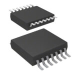 SN74ALVC125DGVR
Compare Hall, shunt, current transformer and Rogowski sensing. Check AC/DC capability, accuracy, isolation, heat and response before selecting a sensor.
Read More
Learn what data acquisition means, from sensors and conditioning to sampling and storage. Review channel timing, wiring, calibration and data quality.
Read More
SN74ALVC125DGVR is listed in the Buffers, Drivers, Receivers, Transceivers range at ChipApex. The manufacturer field lists Texas Instruments. Its product description is IC BUF…
Read More
SN74ALVC125DGVR is listed in the Buffers, Drivers, Receivers, Transceivers range at ChipApex. The manufacturer field lists Texas Instruments. Its product description is IC BUF…
Read More
Choose LED drivers by current, string voltage, dimming and thermal limits. Understand constant-current operation and the checks needed for your load.
Read More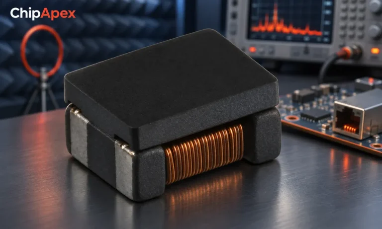
Select a common mode choke using noise frequency, current, insulation and signal integrity. Understand impedance curves, layout and filter limitations.
Read More
SN74ALVC125DGVR is listed in the Buffers, Drivers, Receivers, Transceivers range at ChipApex. The manufacturer field lists Texas Instruments. Its product description is IC BUF…
Read More
SN74ALVC125DGVR is listed in the Buffers, Drivers, Receivers, Transceivers range at ChipApex. The manufacturer field lists Texas Instruments. Its product description is IC BUF…
Read More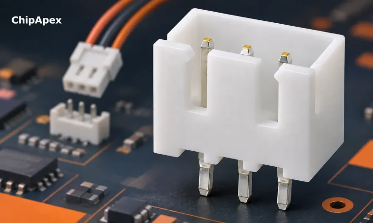
Choose a pin header by pitch, mating geometry, current rating and mounting. Learn why matching pin count and spacing does not guarantee compatibility.
Read More
SN74ALVC125DGVR is listed in the Buffers, Drivers, Receivers, Transceivers range at ChipApex. The manufacturer field lists Texas Instruments. Its product description is IC BUF…
Read More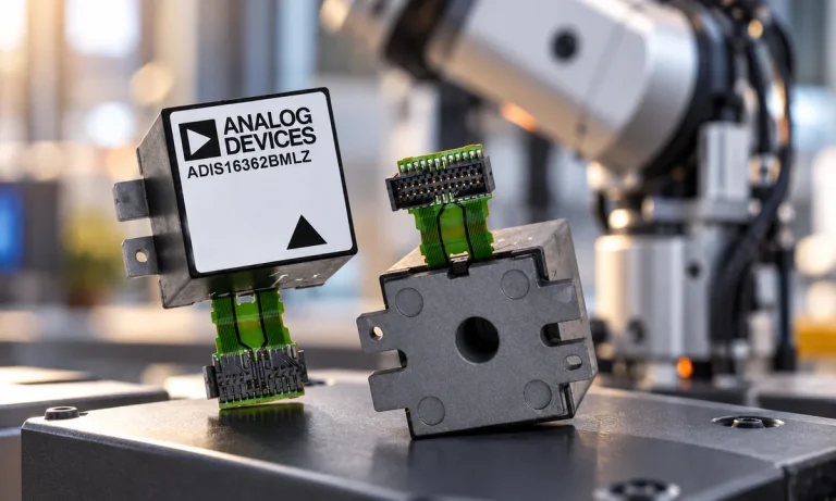
Learn what an IMU measures, how accelerometers and gyroscopes work together, why orientation estimates drift, and what to compare.
Read More
SN74ALVC125DGVR is listed in the Buffers, Drivers, Receivers, Transceivers range at ChipApex. The manufacturer field lists Texas Instruments. Its product description is IC BUF…
Read More
The activity of extra discounts on wholesale prices is in full swing…
Please fill in your contact information and we will send you the latest wholesale price list.





