 ChipApex | Global Electronic Components Supplier

SEARCH
Search Product
Search Post
— IC芯片 | 连接器 | 传感器 | 被动器件 —
Search productSearch post
— IC芯片 | 连接器 | 传感器 | 被动器件 —
Consult the customer manager about the wholesale price.
consultation hotline:86-132-6715-2157
email:[email protected]
Contact the product manager for consultation. One-stop consultation is available.
Do you want a lower wholesale price? Please send us your inquiry and we will reply immediately.
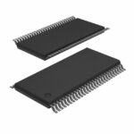
SN74ALVC7814-25DL is listed in the FIFOs Memory range at ChipApex. The manufacturer field lists Texas Instruments. Its product description is IC FIFO ASYNC 64X18 18NS 56SSOP. Review the specifications below when checking this part for your BOM.
The SN74ALVC7814-25DL is a low-power first-in, first-out memory device manufactured by Texas Instruments. It features an 18-bit data bus width and a storage capacity of 1.125 kbit (64 x 18). The component operates within a supply voltage range of 3 V to 3.6 V and supports asynchronous or coincident load and unload clocks. It provides fast access times of 18 ns with a 50-pF load and supports data rates up to 40 MHz. The device includes full, empty, half-full, and programmable almost-full/almost-empty status flags.
Verify that the specific ordering suffix matches the required speed grade and package type. Confirm RoHS compliance and moisture sensitivity level ratings before procurement. Ensure the selected variant aligns with the intended operating temperature range and supply voltage requirements for the target application.
Select this component when an 18-bit wide FIFO buffer is required for low-voltage CMOS applications. Consider the 18 ns access time and 40 MHz maximum frequency for timing constraints. Verify compatibility with existing logic levels and ensure sufficient pin count for the SSOP-56 package fits the design layout.
This part belongs to the SN74ALVC7814 family of low-power advanced CMOS FIFO memories. It is designed for 3-V to 3.6-V operation and offers pin-to-pin compatibility with other members of the Widebus family. The device utilizes shrink small-outline packaging to provide a compact footprint for dense circuit board designs.
The datasheet indicates pin-to-pin compatibility with SN74ACT7804, SN74ACT7806, and SN74ACT7814. Verify voltage level compatibility as these counterparts may operate at different supply voltages compared to the ALVC series.
The offset values are programmed after reset and before the first word is written. The program enable must be held low while the binary value on D0–D7 is latched during the rising edge of the load clock.
When the output-enable signal is high, the Q outputs enter a high-impedance state, effectively disconnecting them from the bus.
Explore related parts through Logic, Integrated Circuits (ICs), all product categories, ChipApex homepage.
 SN74ALVC7814-25DL
SN74ALVC7814-25DL is listed in the FIFOs Memory range at ChipApex. The manufacturer field lists Texas Instruments. Its product description is IC FIFO ASYNC 64X18…
Read More
Understand how a comparator switches at a voltage threshold, why hysteresis prevents chatter, and which output and input specs matter.
Read More
SN74ALVC7814-25DL is listed in the FIFOs Memory range at ChipApex. The manufacturer field lists Texas Instruments. Its product description is IC FIFO ASYNC 64X18…
Read More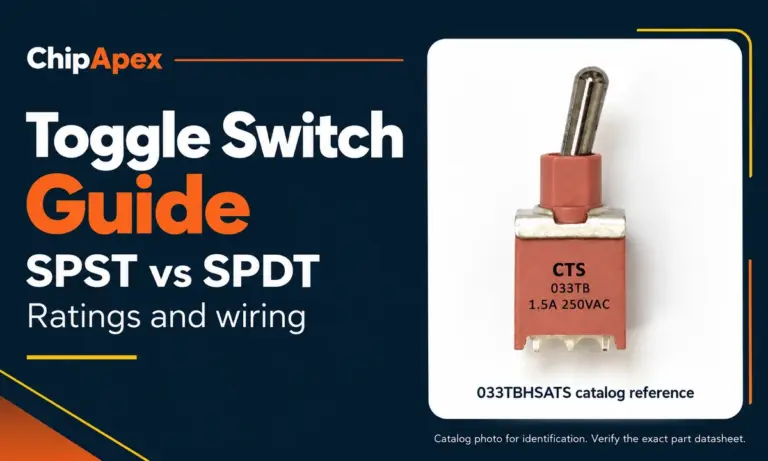
Compare SPST and SPDT toggle switches, understand AC/DC ratings, and follow wiring examples. Check contact action, mounting and parts in the ChipApex catalog.
Read More
Select MOV varistors by continuous voltage, clamping behavior, surge waveform and repetition. Check thermal disconnection, fuse coordination and replacements.
Read More
SN74ALVC7814-25DL is listed in the FIFOs Memory range at ChipApex. The manufacturer field lists Texas Instruments. Its product description is IC FIFO ASYNC 64X18…
Read More
SN74ALVC7814-25DL is listed in the FIFOs Memory range at ChipApex. The manufacturer field lists Texas Instruments. Its product description is IC FIFO ASYNC 64X18…
Read More
SN74ALVC7814-25DL is listed in the FIFOs Memory range at ChipApex. The manufacturer field lists Texas Instruments. Its product description is IC FIFO ASYNC 64X18…
Read More
Choose a DIP switch by contact type, coded positions, footprint and signal ratings. Check logic polarity, assembly conditions and PCB configuration behavior.
Read More
SN74ALVC7814-25DL is listed in the FIFOs Memory range at ChipApex. The manufacturer field lists Texas Instruments. Its product description is IC FIFO ASYNC 64X18…
Read More
SN74ALVC7814-25DL is listed in the FIFOs Memory range at ChipApex. The manufacturer field lists Texas Instruments. Its product description is IC FIFO ASYNC 64X18…
Read More
SN74ALVC7814-25DL is listed in the FIFOs Memory range at ChipApex. The manufacturer field lists Texas Instruments. Its product description is IC FIFO ASYNC 64X18…
Read More
The activity of extra discounts on wholesale prices is in full swing…
Please fill in your contact information and we will send you the latest wholesale price list.





