 ChipApex | Global Electronic Components Supplier

SEARCH
Search Product
Search Post
— IC芯片 | 连接器 | 传感器 | 被动器件 —
Search productSearch post
— IC芯片 | 连接器 | 传感器 | 被动器件 —
Consult the customer manager about the wholesale price.
consultation hotline:86-132-6715-2157
email:[email protected]
Contact the product manager for consultation. One-stop consultation is available.
Do you want a lower wholesale price? Please send us your inquiry and we will reply immediately.
SN74HC241PW is listed in the Buffers, Drivers, Receivers, Transceivers range at ChipApex. The manufacturer field lists Texas Instruments. Its product description is IC BUFFER NON-INVERT 6V 20TSSOP. Review the specifications below when checking this part for your BOM.
The SN74HC241PW is an octal buffer and line driver with 3-state outputs manufactured by Texas Instruments. It operates within a supply voltage range of 2 V to 6 V. The device features high-current outputs capable of driving up to 15 LSTTL loads, with typical propagation delay of 11 ns at 4.5 V. It consumes low power, with maximum ICC of 80 μA. The component is housed in a 20-pin TSSOP package.
Verify the specific ordering suffix and package type against the manufacturer's current orderable addendum. Confirm RoHS compliance status and moisture sensitivity level ratings prior to procurement. Ensure the selected variant matches the required operating temperature range and thermal resistance specifications for the intended application environment.
Select this component when designing systems requiring octal buffering with 3-state capabilities. Consider the 2 V to 6 V operating voltage range and the requirement for separate output-enable controls. Evaluate the thermal performance characteristics associated with the TSSOP-20 package for adequate heat dissipation in the target circuit design.
This part belongs to the SNx4HC241 family of octal buffers and line drivers with 3-state outputs. The 'HC' designation indicates High-speed CMOS technology. The PW suffix specifically denotes the TSSOP (Thin Shrink Small Outline Package) with 20 pins, distinguishing it from other package options like SOIC or PDIP available within the same logical family.
SN74HC241PWR is an active production alternative in the same TSSOP-20 package. Other package variants such as SN74HC241DW (SOIC) or SN74HC241N (PDIP) offer functional equivalence but require different footprint considerations on the printed circuit board.
The device is organized as two 4-bit buffers with separate output-enable inputs (1OE and 2OE). When an enable input is low, the respective outputs pass non-inverted data; when high, they enter a high-impedance state.
A 0.1-μF capacitor is recommended for each VCC terminal to prevent power disturbance. It should be installed as close to the power terminal as possible.
Explore related parts through Logic, Integrated Circuits (ICs), all product categories, ChipApex homepage.
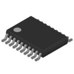 SN74HC241PW

SN74HC241PW is listed in the Buffers, Drivers, Receivers, Transceivers range at ChipApex. The manufacturer field lists Texas Instruments. Its product description is IC BUFFER…
Read More
SN74HC241PW is listed in the Buffers, Drivers, Receivers, Transceivers range at ChipApex. The manufacturer field lists Texas Instruments. Its product description is IC BUFFER…
Read More
SN74HC241PW is listed in the Buffers, Drivers, Receivers, Transceivers range at ChipApex. The manufacturer field lists Texas Instruments. Its product description is IC BUFFER…
Read More
SN74HC241PW is listed in the Buffers, Drivers, Receivers, Transceivers range at ChipApex. The manufacturer field lists Texas Instruments. Its product description is IC BUFFER…
Read More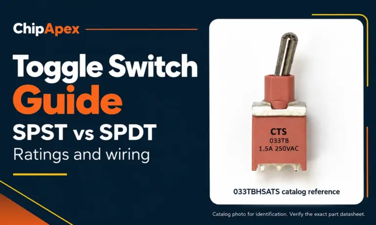
Compare SPST and SPDT toggle switches, understand AC/DC ratings, and follow wiring examples. Check contact action, mounting and parts in the ChipApex catalog.
Read More
SN74HC241PW is listed in the Buffers, Drivers, Receivers, Transceivers range at ChipApex. The manufacturer field lists Texas Instruments. Its product description is IC BUFFER…
Read More
SN74HC241PW is listed in the Buffers, Drivers, Receivers, Transceivers range at ChipApex. The manufacturer field lists Texas Instruments. Its product description is IC BUFFER…
Read More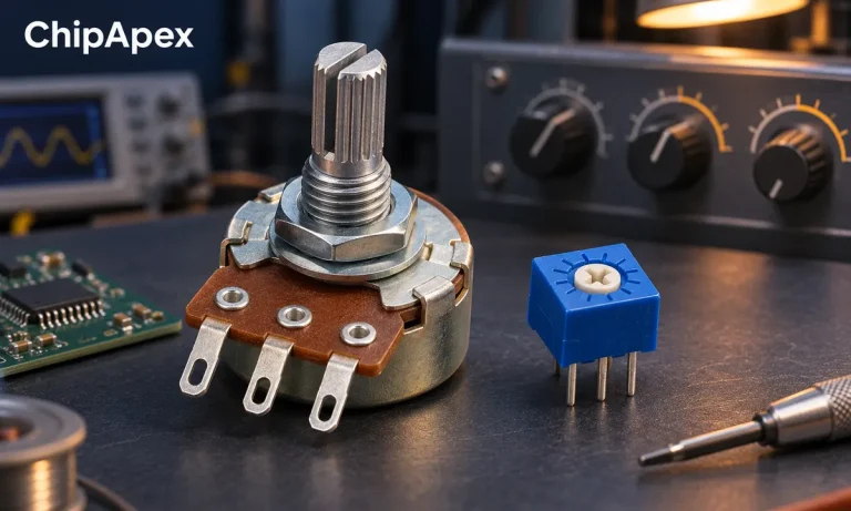
Compare rheostat and potentiometer wiring and functions. Understand divider loading, wiper current, track power and practical component selection.
Read More
SN74HC241PW is listed in the Buffers, Drivers, Receivers, Transceivers range at ChipApex. The manufacturer field lists Texas Instruments. Its product description is IC BUFFER…
Read More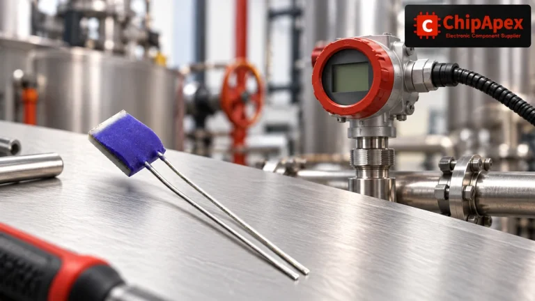
Compare Pt100 and Pt1000 RTDs, two-, three- and four-wire connections, excitation and self-heating. Build an error budget from element to reported temperature.
Read More
SN74HC241PW is listed in the Buffers, Drivers, Receivers, Transceivers range at ChipApex. The manufacturer field lists Texas Instruments. Its product description is IC BUFFER…
Read More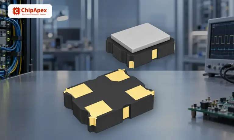
Understand how oscillators generate timing signals, how they differ from crystals, and which frequency, output and stability specs matter when choosing one.
Read More
The activity of extra discounts on wholesale prices is in full swing…
Please fill in your contact information and we will send you the latest wholesale price list.





