ChipApex | Global Electronic Components Supplier

SEARCH
Search Product
Search Post
— IC芯片 | 连接器 | 传感器 | 被动器件 —
Search productSearch post
— IC芯片 | 连接器 | 传感器 | 被动器件 —
Consult the customer manager about the wholesale price.
consultation hotline:86-132-6715-2157
email:[email protected]
Contact the product manager for consultation. One-stop consultation is available.
Do you want a lower wholesale price? Please send us your inquiry and we will reply immediately.
SN74HCS264QDRQ1 is listed in the Shift Registers range at ChipApex. The manufacturer field lists Texas Instruments. Its product description is AUTOMOTIVE 8-BIT PARALLEL-OUT SE. Review the specifications below when checking this part for your BOM.
The SN74HCS264QDRQ1 is an automotive-grade, 8-bit parallel-out serial shift register featuring Schmitt-trigger inputs and inverted outputs. It operates within a supply voltage range of 2 V to 6 V and supports temperatures from -40°C to +125°C. The device utilizes AND-gated serial inputs (A and B) with an asynchronous clear function. Data propagates on the rising edge of the clock signal. It provides balanced CMOS push-pull outputs capable of ±7.8 mA drive current at 6 V.
Verify the specific ordering suffix matches the required package type, as the SN74HCS264-Q1 family includes multiple options such as TSSOP and SOIC. Confirm that the QDRQ1 designation aligns with your manufacturing assembly requirements. Ensure the component meets AEC-Q100 Grade 1 specifications for your target automotive environment. Review the datasheet for absolute maximum ratings to prevent damage during handling and operation.
Select this component when an 8-bit shift register with inverted outputs and Schmitt-trigger inputs is required for automotive systems. The AND-gated serial input design simplifies logic control by requiring two inputs to activate the data line. Consider the wide operating voltage range of 2 V to 6 V for compatibility with various power rails. Verify that the SOIC-16 package fits your PCB layout constraints and thermal management needs.
This device belongs to the SN74HCS-Q1 family of automotive HCMOS logic components. It shares the HCS series characteristics, including Schmitt-trigger inputs and low power consumption. The part is designed for robust performance in electrically noisy automotive environments. It complements other logic gates and drivers within the same automotive qualification standard.
Check for SN74HCS264PW-Q1 if a TSSOP package is preferred over the SOIC format. Verify functional equivalence regarding the inverted output state and AND-gated serial inputs before substitution.
Data is only accepted into the first stage of the shift register when both serial inputs A and B are high. If either input is low, the first stage stores a low value.
All outputs are inverted from the data stored in the respective registers. For example, if a register stores a high value, the corresponding output will be low.
Yes, data at the serial inputs can be changed while CLK is high or low, provided the minimum setup time requirements are met before the rising clock edge.
Explore related parts through Logic, Integrated Circuits (ICs), all product categories, ChipApex homepage.
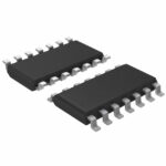 SN74HCS264QDRQ1
SN74HCS264QDRQ1 is listed in the Shift Registers range at ChipApex. The manufacturer field lists Texas Instruments. Its product description is AUTOMOTIVE 8-BIT PARALLEL-OUT SE.…
Read More
SN74HCS264QDRQ1 is listed in the Shift Registers range at ChipApex. The manufacturer field lists Texas Instruments. Its product description is AUTOMOTIVE 8-BIT PARALLEL-OUT SE.…
Read More
SN74HCS264QDRQ1 is listed in the Shift Registers range at ChipApex. The manufacturer field lists Texas Instruments. Its product description is AUTOMOTIVE 8-BIT PARALLEL-OUT SE.…
Read More
Understand voltage controlled oscillator tuning, phase noise and PLL operation. Check supply noise, output loading and requirements before selection.
Read More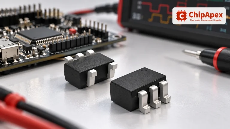
Choose logic inverter ICs by thresholds, supply, output drive and delay. Compare standard and Schmitt-trigger inputs, power sequencing and replacement checks.
Read MoreSN74HCS264QDRQ1 is listed in the Shift Registers range at ChipApex. The manufacturer field lists Texas Instruments. Its product description is AUTOMOTIVE 8-BIT PARALLEL-OUT SE.…
Read More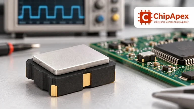
Compare RC, crystal and MEMS oscillator circuits. Check ppm, jitter, load capacitance, startup margin and output compatibility before choosing a clock source.
Read More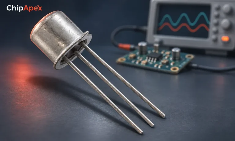
Learn what a transistor does in a circuit. Compare switching and amplification, BJT and MOSFET drive, operating limits and practical component selection.
Read More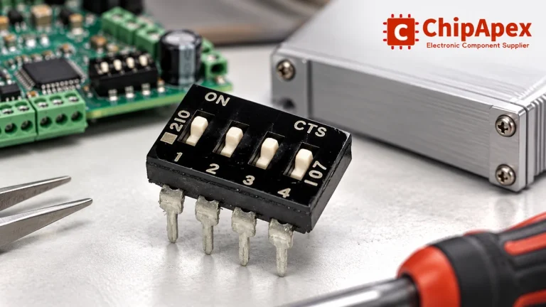
Choose a DIP switch by contact type, coded positions, footprint and signal ratings. Check logic polarity, assembly conditions and PCB configuration behavior.
Read More
SN74HCS264QDRQ1 is listed in the Shift Registers range at ChipApex. The manufacturer field lists Texas Instruments. Its product description is AUTOMOTIVE 8-BIT PARALLEL-OUT SE.…
Read More
SN74HCS264QDRQ1 is listed in the Shift Registers range at ChipApex. The manufacturer field lists Texas Instruments. Its product description is AUTOMOTIVE 8-BIT PARALLEL-OUT SE.…
Read More
SN74HCS264QDRQ1 is listed in the Shift Registers range at ChipApex. The manufacturer field lists Texas Instruments. Its product description is AUTOMOTIVE 8-BIT PARALLEL-OUT SE.…
Read More
The activity of extra discounts on wholesale prices is in full swing…
Please fill in your contact information and we will send you the latest wholesale price list.