 ChipApex | Global Electronic Components Supplier

SEARCH
Search Product
Search Post
— IC芯片 | 连接器 | 传感器 | 被动器件 —
Search productSearch post
— IC芯片 | 连接器 | 传感器 | 被动器件 —
Consult the customer manager about the wholesale price.
consultation hotline:86-132-6715-2157
email:[email protected]
Contact the product manager for consultation. One-stop consultation is available.
Do you want a lower wholesale price? Please send us your inquiry and we will reply immediately.
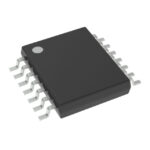
SN74LV126APW is listed in the Buffers, Drivers, Receivers, Transceivers range at ChipApex. The manufacturer field lists Texas Instruments. Its product description is IC BUF NON-INVERT 5.5V 14TSSOP. Review the specifications below when checking this part for your BOM.
The SN74LV126APW is a quadruple bus buffer gate with 3-state outputs manufactured by Texas Instruments. It operates within a supply voltage range of 2V to 5.5V and features independent line drivers for each channel. The device supports mixed-mode voltage operation, allowing inputs to accept voltages up to 5.5V regardless of the VCC level. It includes Ioff support for live insertion and partial power down modes. The component is housed in a 14-pin TSSOP package.
Verify the specific ordering suffix against the manufacturer's latest Package Option Addendum to confirm production status and material compliance. The 'PW' designation indicates a TSSOP-14 package. Confirm RoHS status and moisture sensitivity level ratings prior to assembly planning. Ensure the selected variant matches the required lead finish and reel specifications for surface-mount placement processes.
Select this component when designing bus interfaces requiring low-drive CMOS characteristics to minimize output ringing and overshoot. It is suitable for applications where balanced output drive and slow edge rates are preferred to reduce electromagnetic interference. Verify that the load capacitance and transition rates remain within the specified limits for the chosen operating voltage to ensure signal integrity.
This part belongs to the SN74LV126A family of quadruple bus buffer gates. It shares functional similarities with other LV logic series devices but is distinguished by its specific voltage tolerance and 3-state control architecture. The PW suffix identifies the physical TSSOP packaging format used for surface-mount technology integration.
SN74LV126APWR
To ensure the high-impedance state during power-up or power-down, the Output Enable (OE) pin should be tied to GND through a pulldown resistor. The minimum resistor value is determined by the current-sourcing capability of the driver.
The inputs are 5.5V tolerant at any valid VCC, making the device suitable for translating signals down to lower voltage domains while accepting 5.5V inputs.
Explore related parts through Logic, Integrated Circuits (ICs), all product categories, ChipApex homepage.
 SN74LV126APW
SN74LV126APW is listed in the Buffers, Drivers, Receivers, Transceivers range at ChipApex. The manufacturer field lists Texas Instruments. Its product description is IC BUF…
Read More
Compare Pt100 and Pt1000 RTDs, two-, three- and four-wire connections, excitation and self-heating. Build an error budget from element to reported temperature.
Read More
SN74LV126APW is listed in the Buffers, Drivers, Receivers, Transceivers range at ChipApex. The manufacturer field lists Texas Instruments. Its product description is IC BUF…
Read More
SN74LV126APW is listed in the Buffers, Drivers, Receivers, Transceivers range at ChipApex. The manufacturer field lists Texas Instruments. Its product description is IC BUF…
Read More
SN74LV126APW is listed in the Buffers, Drivers, Receivers, Transceivers range at ChipApex. The manufacturer field lists Texas Instruments. Its product description is IC BUF…
Read More
SN74LV126APW is listed in the Buffers, Drivers, Receivers, Transceivers range at ChipApex. The manufacturer field lists Texas Instruments. Its product description is IC BUF…
Read More
Learn how to use ferrite beads for noise filtering. Check impedance, DC bias, placement, resonance and load-step behavior before selecting a part.
Read More
SN74LV126APW is listed in the Buffers, Drivers, Receivers, Transceivers range at ChipApex. The manufacturer field lists Texas Instruments. Its product description is IC BUF…
Read More
SN74LV126APW is listed in the Buffers, Drivers, Receivers, Transceivers range at ChipApex. The manufacturer field lists Texas Instruments. Its product description is IC BUF…
Read More
SN74LV126APW is listed in the Buffers, Drivers, Receivers, Transceivers range at ChipApex. The manufacturer field lists Texas Instruments. Its product description is IC BUF…
Read More
SN74LV126APW is listed in the Buffers, Drivers, Receivers, Transceivers range at ChipApex. The manufacturer field lists Texas Instruments. Its product description is IC BUF…
Read More
SN74LV126APW is listed in the Buffers, Drivers, Receivers, Transceivers range at ChipApex. The manufacturer field lists Texas Instruments. Its product description is IC BUF…
Read More
The activity of extra discounts on wholesale prices is in full swing…
Please fill in your contact information and we will send you the latest wholesale price list.





