 ChipApex | Global Electronic Components Supplier

SEARCH
Search Product
Search Post
— IC芯片 | 连接器 | 传感器 | 被动器件 —
Search productSearch post
— IC芯片 | 连接器 | 传感器 | 被动器件 —
Consult the customer manager about the wholesale price.
consultation hotline:86-132-6715-2157
email:[email protected]
Contact the product manager for consultation. One-stop consultation is available.
Do you want a lower wholesale price? Please send us your inquiry and we will reply immediately.
SN74LV367APWRG4 is listed in the Buffers, Drivers, Receivers, Transceivers range at ChipApex. The manufacturer field lists Texas Instruments. Its product description is IC BUF NON-INVERT 5.5V 16TSSOP. Review the specifications below when checking this part for your BOM.
The SN74LV367APWRG4 is a hex buffer and line driver with three-state outputs manufactured by Texas Instruments. It operates within a supply voltage range of 2 V to 5.5 V, utilizing CMOS logic technology. The device features six non-inverting input lines and six corresponding output lines housed in a 16-pin TSSOP package. Key electrical characteristics include a maximum low-level output current of 24 mA and a high-level output current of -24 mA. The static power consumption is typically 20 µA, with an operating temperature range spanning from -40°C to +85°C.
Verify the complete part number including the suffix G4 to ensure compliance with RoHS directives and lead-free manufacturing standards. Confirm the package type matches the design footprint requirements. Cross-reference the datasheet revision date to ensure alignment with current electrical specifications and pinout definitions before finalizing procurement orders.
Select this component when designing systems requiring hex buffering with three-state control under varying voltage conditions. Ensure the load capacitance and drive current requirements fall within the specified limits of the LV series. Consider the thermal performance of the TSSOP package relative to the ambient operating environment and board layout constraints.
This device belongs to the SN74LV367A family of logic integrated circuits produced by Texas Instruments. It is part of the broader Low-Voltage CMOS logic portfolio designed for high-speed digital applications. The 'G4' suffix indicates environmental compliance, specifically adhering to European Union restrictions on hazardous substances in electronic equipment.
The device includes two enable inputs that control the three-state outputs. When asserted, they allow the buffered signals to pass through; otherwise, the outputs enter a high-impedance state.
The SN74LV367APWRG4 provides non-inverting buffering, meaning the output signal follows the input signal phase without inversion.
Explore related parts through Logic, Integrated Circuits (ICs), all product categories, ChipApex homepage.
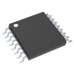 SN74LV367APWRG4
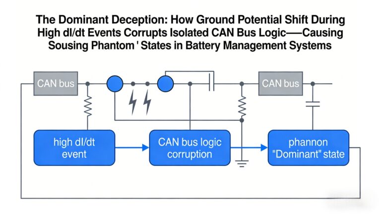
SN74LV367APWRG4 is listed in the Buffers, Drivers, Receivers, Transceivers range at ChipApex. The manufacturer field lists Texas Instruments. Its product description is IC BUF…
Read More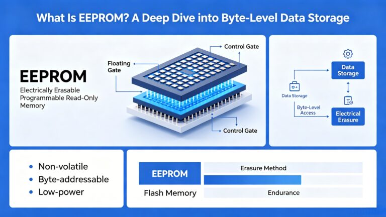
SN74LV367APWRG4 is listed in the Buffers, Drivers, Receivers, Transceivers range at ChipApex. The manufacturer field lists Texas Instruments. Its product description is IC BUF…
Read More
See how a MEMS gyroscope measures angular rate, why its angle estimate drifts, and which range, noise, interface and temperature specs to compare.
Read More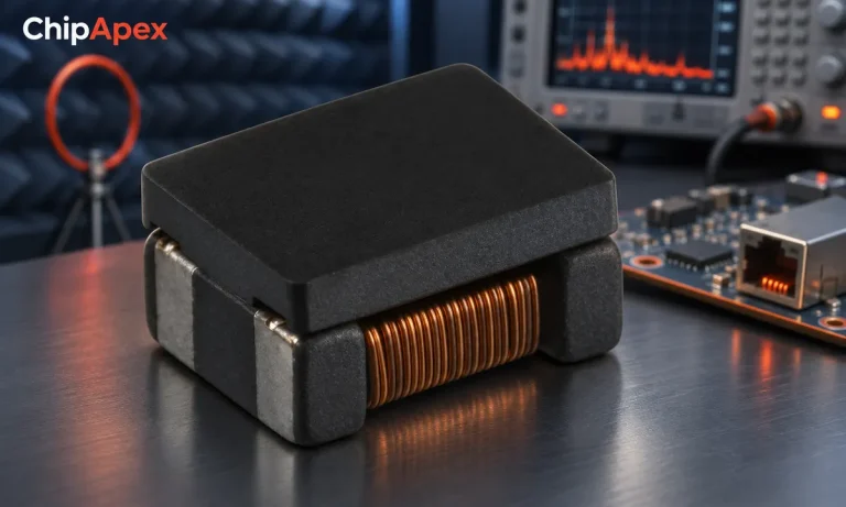
Select a common mode choke using noise frequency, current, insulation and signal integrity. Understand impedance curves, layout and filter limitations.
Read More
Learn how a JFET works and how to compare bias, leakage, noise and pinout. Review practical selection questions for high-impedance analog circuits.
Read More
SN74LV367APWRG4 is listed in the Buffers, Drivers, Receivers, Transceivers range at ChipApex. The manufacturer field lists Texas Instruments. Its product description is IC BUF…
Read More
SN74LV367APWRG4 is listed in the Buffers, Drivers, Receivers, Transceivers range at ChipApex. The manufacturer field lists Texas Instruments. Its product description is IC BUF…
Read More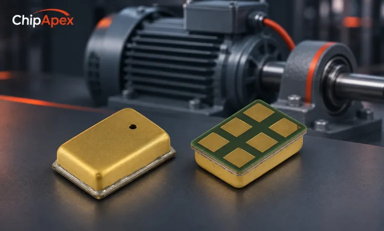
Choose a vibration sensor for machine monitoring. Compare sensing methods, bandwidth, noise and mounting, then define the signal-chain requirements.
Read More
SN74LV367APWRG4 is listed in the Buffers, Drivers, Receivers, Transceivers range at ChipApex. The manufacturer field lists Texas Instruments. Its product description is IC BUF…
Read More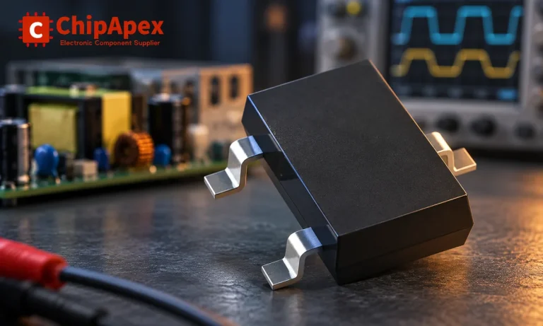
Learn how rectifiers convert AC to DC, compare half-wave and bridge circuits, and select voltage, current, recovery and thermal ratings for your design.
Read More
SN74LV367APWRG4 is listed in the Buffers, Drivers, Receivers, Transceivers range at ChipApex. The manufacturer field lists Texas Instruments. Its product description is IC BUF…
Read More
SN74LV367APWRG4 is listed in the Buffers, Drivers, Receivers, Transceivers range at ChipApex. The manufacturer field lists Texas Instruments. Its product description is IC BUF…
Read More
The activity of extra discounts on wholesale prices is in full swing…
Please fill in your contact information and we will send you the latest wholesale price list.





