 ChipApex | Global Electronic Components Supplier

SEARCH
Search Product
Search Post
— IC芯片 | 连接器 | 传感器 | 被动器件 —
Search productSearch post
— IC芯片 | 连接器 | 传感器 | 被动器件 —
Consult the customer manager about the wholesale price.
consultation hotline:86-132-6715-2157
email:[email protected]
Contact the product manager for consultation. One-stop consultation is available.
Do you want a lower wholesale price? Please send us your inquiry and we will reply immediately.
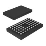
SN74LVC16245AGQLR is listed in the Buffers, Drivers, Receivers, Transceivers range at ChipApex. The manufacturer field lists Texas Instruments. Its product description is IC TXRX NON-INVERT 3.6V 56BGA. Review the specifications below when checking this part for your BOM.
The SN74LVC16245AGQLR is a 16-bit bus transceiver with 3-state outputs from the Texas Instruments Widebus family. It operates on a supply voltage range of 1.65 V to 3.6 V and features inputs tolerant to 5.5 V, supporting mixed-mode signal operation. The device provides asynchronous communication between data buses with a maximum propagation delay of 4 ns at 3.3 V. It includes Ioff circuitry for partial-power-down mode and back-drive protection. ESD protection exceeds JESD 22 standards, rated at 2000 V for the human-body model. It is housed in a 56-ball GQL package.
Verify the specific GQL package configuration against the target PCB footprint. Confirm that the 5.5 V input tolerance aligns with the source logic levels in the design. Ensure proper pull-up resistor implementation on the OE pin to maintain isolation during power cycles. Validate thermal management requirements for the intended operating temperature range.
Select this component when designing systems requiring 16-bit bidirectional data transfer across different voltage domains. It is suitable for applications needing down-voltage translation from 5 V to lower logic levels. Consider its wide operating voltage range and high drive capability for driving multiple loads or long traces in industrial environments.
This part belongs to the SN74LVC16245A series, designed for asynchronous communication between data buses. It functions as either two 8-bit transceivers or one 16-bit transceiver. The device minimizes external timing requirements through its control-function implementation, making it efficient for complex digital interfaces.
SN74LVC16245ADGGR
The device utilizes Ioff circuitry which automatically disables the outputs when powered down. This prevents damaging current backflow through the device when VCC is zero.
The OE input disables the device, effectively isolating the buses. To ensure the high-impedance state during power up or power down, OE should be tied to VCC through a pullup resistor.
Explore related parts through Logic, Integrated Circuits (ICs), all product categories, ChipApex homepage.
 SN74LVC16245AGQLR

SN74LVC16245AGQLR is listed in the Buffers, Drivers, Receivers, Transceivers range at ChipApex. The manufacturer field lists Texas Instruments. Its product description is IC TXRX…
Read More
SN74LVC16245AGQLR is listed in the Buffers, Drivers, Receivers, Transceivers range at ChipApex. The manufacturer field lists Texas Instruments. Its product description is IC TXRX…
Read More
SN74LVC16245AGQLR is listed in the Buffers, Drivers, Receivers, Transceivers range at ChipApex. The manufacturer field lists Texas Instruments. Its product description is IC TXRX…
Read More
SN74LVC16245AGQLR is listed in the Buffers, Drivers, Receivers, Transceivers range at ChipApex. The manufacturer field lists Texas Instruments. Its product description is IC TXRX…
Read More
SN74LVC16245AGQLR is listed in the Buffers, Drivers, Receivers, Transceivers range at ChipApex. The manufacturer field lists Texas Instruments. Its product description is IC TXRX…
Read More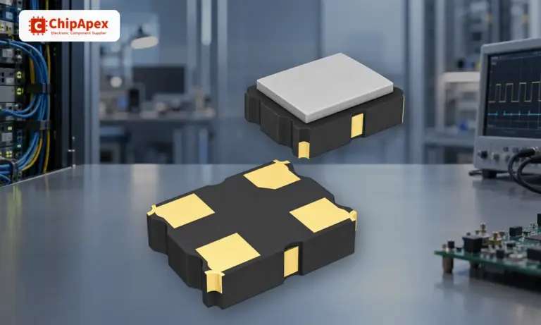
Understand how oscillators generate timing signals, how they differ from crystals, and which frequency, output and stability specs matter when choosing one.
Read More
SN74LVC16245AGQLR is listed in the Buffers, Drivers, Receivers, Transceivers range at ChipApex. The manufacturer field lists Texas Instruments. Its product description is IC TXRX…
Read More
SN74LVC16245AGQLR is listed in the Buffers, Drivers, Receivers, Transceivers range at ChipApex. The manufacturer field lists Texas Instruments. Its product description is IC TXRX…
Read More
SN74LVC16245AGQLR is listed in the Buffers, Drivers, Receivers, Transceivers range at ChipApex. The manufacturer field lists Texas Instruments. Its product description is IC TXRX…
Read More
SN74LVC16245AGQLR is listed in the Buffers, Drivers, Receivers, Transceivers range at ChipApex. The manufacturer field lists Texas Instruments. Its product description is IC TXRX…
Read More
SN74LVC16245AGQLR is listed in the Buffers, Drivers, Receivers, Transceivers range at ChipApex. The manufacturer field lists Texas Instruments. Its product description is IC TXRX…
Read More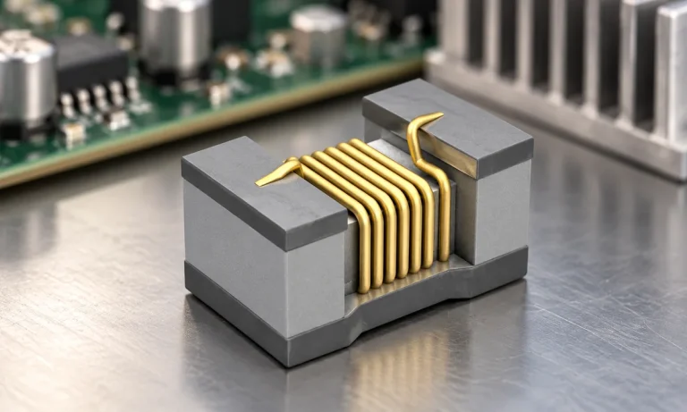
See when an inductor behaves linearly, how DC bias and saturation reduce inductance, and which current and temperature curves to check.
Read More
The activity of extra discounts on wholesale prices is in full swing…
Please fill in your contact information and we will send you the latest wholesale price list.





