 ChipApex | Global Electronic Components Supplier

SEARCH
Search Product
Search Post
— IC芯片 | 连接器 | 传感器 | 被动器件 —
Search productSearch post
— IC芯片 | 连接器 | 传感器 | 被动器件 —
Consult the customer manager about the wholesale price.
consultation hotline:86-132-6715-2157
email:[email protected]
Contact the product manager for consultation. One-stop consultation is available.
Do you want a lower wholesale price? Please send us your inquiry and we will reply immediately.
SN74LVC1G79DCKT is listed in the Flip Flops range at ChipApex. The manufacturer field lists Texas Instruments. Its product description is IC FF D-TYPE SNGL 1BIT SC70-5. Review the specifications below when checking this part for your BOM.
The SN74LVC1G79DCKT is a single positive-edge-triggered D-type flip-flop from Texas Instruments, housed in a SC-70-5 NanoFree package. It operates within a supply voltage range of 1.65 V to 5.5 V and supports CMOS and TTL input types. The device features non-inverting output polarity with a maximum propagation delay of 5 ns. Output drive capability reaches ±32 mA, while static current consumption remains low at 10 µA maximum. It functions reliably across an operating temperature range starting from -40°C.
Verify the specific ordering suffix 'RG4' or 'T' against the required tape-and-reel quantity and RoHS compliance status. Confirm that the SC-70-5 package dimensions align with PCB footprint constraints. Ensure the selected variant matches the intended voltage level shifting requirements for the target application environment.
Select this component when a compact, single-bit storage element is required for high-speed digital logic applications. The LVC series offers compatibility with both 1.65 V and 5.5 V systems, facilitating interface between different voltage domains. Consider the SC-70-5 package for space-constrained designs requiring surface-mount technology integration.
This part belongs to the SN74LVC1Gxx family of single-function logic devices designed for low-voltage CMOS operations. The LVC series emphasizes low power consumption and high speed, making it suitable for portable and battery-operated devices. The D-type flip-flop configuration provides essential data storage capabilities in sequential logic circuits.
The Ioff circuit automatically disables the outputs when the device is powered down, preventing backflow current that could damage the component or interfere with other active parts of the system.
Data present at the D input is transferred to the Q output specifically on the positive edge of the clock pulse, provided setup and hold time requirements are met.
Explore related parts through Logic, Integrated Circuits (ICs), all product categories, ChipApex homepage.
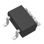 SN74LVC1G79DCKT
Understand how a comparator switches at a voltage threshold, why hysteresis prevents chatter, and which output and input specs matter.
Read More
SN74LVC1G79DCKT is listed in the Flip Flops range at ChipApex. The manufacturer field lists Texas Instruments. Its product description is IC FF D-TYPE SNGL…
Read More
Learn what an integrated circuit is, how ICs work, the main types and the specs to check before choosing a part for your design…
Read More
SN74LVC1G79DCKT is listed in the Flip Flops range at ChipApex. The manufacturer field lists Texas Instruments. Its product description is IC FF D-TYPE SNGL…
Read More
SN74LVC1G79DCKT is listed in the Flip Flops range at ChipApex. The manufacturer field lists Texas Instruments. Its product description is IC FF D-TYPE SNGL…
Read More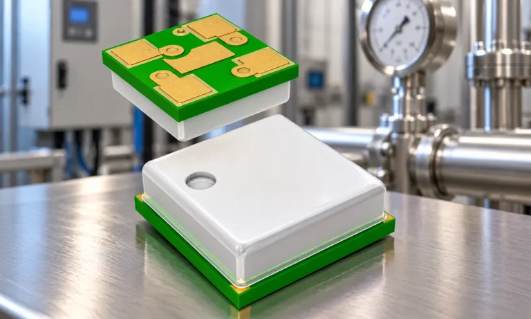
Learn how a pressure transducer converts pressure into voltage, current, or digital output, and compare pressure references and key selection specs.
Read More
SN74LVC1G79DCKT is listed in the Flip Flops range at ChipApex. The manufacturer field lists Texas Instruments. Its product description is IC FF D-TYPE SNGL…
Read More
SN74LVC1G79DCKT is listed in the Flip Flops range at ChipApex. The manufacturer field lists Texas Instruments. Its product description is IC FF D-TYPE SNGL…
Read More
SN74LVC1G79DCKT is listed in the Flip Flops range at ChipApex. The manufacturer field lists Texas Instruments. Its product description is IC FF D-TYPE SNGL…
Read More
Learn what an IMU measures, how accelerometers and gyroscopes work together, why orientation estimates drift, and what to compare.
Read More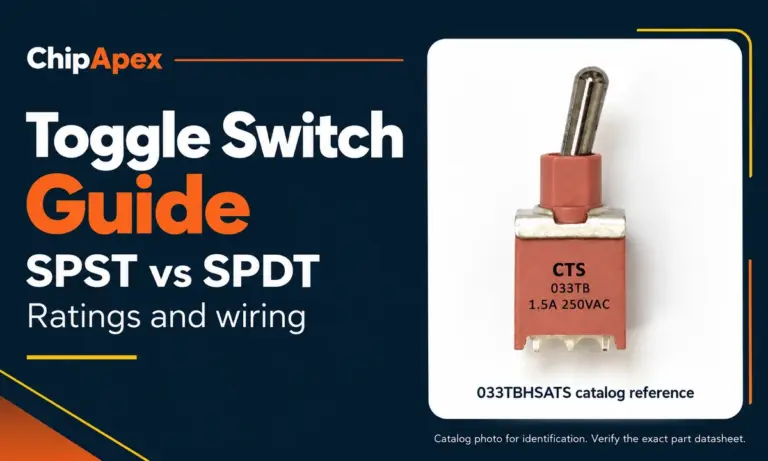
Compare SPST and SPDT toggle switches, understand AC/DC ratings, and follow wiring examples. Check contact action, mounting and parts in the ChipApex catalog.
Read More
SN74LVC1G79DCKT is listed in the Flip Flops range at ChipApex. The manufacturer field lists Texas Instruments. Its product description is IC FF D-TYPE SNGL…
Read More
The activity of extra discounts on wholesale prices is in full swing…
Please fill in your contact information and we will send you the latest wholesale price list.





