 ChipApex | Global Electronic Components Supplier

SEARCH
Search Product
Search Post
— IC芯片 | 连接器 | 传感器 | 被动器件 —
Search productSearch post
— IC芯片 | 连接器 | 传感器 | 被动器件 —
Consult the customer manager about the wholesale price.
consultation hotline:86-132-6715-2157
email:[email protected]
Contact the product manager for consultation. One-stop consultation is available.
Do you want a lower wholesale price? Please send us your inquiry and we will reply immediately.
SN74LVCZ240APW is listed in the Buffers, Drivers, Receivers, Transceivers range at ChipApex. The manufacturer field lists Texas Instruments. Its product description is IC BUFFER INVERT 3.6V 20TSSOP. Review the specifications below when checking this part for your BOM.
The SN74LVCZ240A is an octal buffer with Schmitt-trigger inputs and 3-state outputs, manufactured by Texas Instruments. It operates from a supply voltage of 2.7V to 3.6V. The device features balanced CMOS outputs capable of sinking and sourcing similar currents. Inputs accept voltages up to 5.5V, supporting mixed-mode signal operation with 3.3V VCC. Maximum propagation delay is 6.5ns at 3.3V. Typical output ground bounce is 2V at VCC = 3.3V. Latch-up performance exceeds 100mA per JESD 78.
Verify the specific package variant (PW, DW, or NS) required for the design, as dimensions differ. Confirm that the application environment stays within the -40°C to +85°C operating temperature range. Ensure input signals do not exceed the absolute maximum ratings to prevent damage. Check for updated documentation revisions before finalizing the bill of materials.
Select this component when 3.3V logic interfaces with 5V tolerant systems are required. The balanced output drive supports high-speed digital signaling. Verify that the load capacitance does not exceed 50pF to maintain specified switching characteristics. Consider the thermal metrics if multiple devices operate simultaneously in enclosed spaces.
This device belongs to the SN74LVCZ family, designed for low-voltage applications. It provides octal buffering capabilities with independent control over two banks of four drivers each. The inclusion of Schmitt triggers enhances signal integrity in noisy environments compared to standard CMOS buffers.
SN74LVC240ADW
Both OE pins must be tied to VCC through a pull-up resistor to confirm the high-impedance state during power-up or power-down.
The device disables all outputs regardless of input voltages, preventing current sourcing or sinking, defined by the Ioff specification.
Explore related parts through Logic, Integrated Circuits (ICs), all product categories, ChipApex homepage.
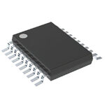 SN74LVCZ240APW
SN74LVCZ240APW is listed in the Buffers, Drivers, Receivers, Transceivers range at ChipApex. The manufacturer field lists Texas Instruments. Its product description is IC BUFFER…
Read More
SN74LVCZ240APW is listed in the Buffers, Drivers, Receivers, Transceivers range at ChipApex. The manufacturer field lists Texas Instruments. Its product description is IC BUFFER…
Read More
SN74LVCZ240APW is listed in the Buffers, Drivers, Receivers, Transceivers range at ChipApex. The manufacturer field lists Texas Instruments. Its product description is IC BUFFER…
Read More
SN74LVCZ240APW is listed in the Buffers, Drivers, Receivers, Transceivers range at ChipApex. The manufacturer field lists Texas Instruments. Its product description is IC BUFFER…
Read More
SN74LVCZ240APW is listed in the Buffers, Drivers, Receivers, Transceivers range at ChipApex. The manufacturer field lists Texas Instruments. Its product description is IC BUFFER…
Read More
Choose a DIP switch by contact type, coded positions, footprint and signal ratings. Check logic polarity, assembly conditions and PCB configuration behavior.
Read More
SN74LVCZ240APW is listed in the Buffers, Drivers, Receivers, Transceivers range at ChipApex. The manufacturer field lists Texas Instruments. Its product description is IC BUFFER…
Read More
SN74LVCZ240APW is listed in the Buffers, Drivers, Receivers, Transceivers range at ChipApex. The manufacturer field lists Texas Instruments. Its product description is IC BUFFER…
Read More
Select MOV varistors by continuous voltage, clamping behavior, surge waveform and repetition. Check thermal disconnection, fuse coordination and replacements.
Read More
Learn what an IMU measures, how accelerometers and gyroscopes work together, why orientation estimates drift, and what to compare.
Read More
Choose an AC to DC converter by input range, output demand, isolation, efficiency and thermal derating. Compare architectures and check installation needs.
Read More
SN74LVCZ240APW is listed in the Buffers, Drivers, Receivers, Transceivers range at ChipApex. The manufacturer field lists Texas Instruments. Its product description is IC BUFFER…
Read More
The activity of extra discounts on wholesale prices is in full swing…
Please fill in your contact information and we will send you the latest wholesale price list.





