ChipApex | Global Electronic Components Supplier

SEARCH
Search Product
Search Post
— IC芯片 | 连接器 | 传感器 | 被动器件 —
Search productSearch post
— IC芯片 | 连接器 | 传感器 | 被动器件 —
Consult the customer manager about the wholesale price.
consultation hotline:86-132-6715-2157
email:[email protected]
Contact the product manager for consultation. One-stop consultation is available.
Do you want a lower wholesale price? Please send us your inquiry and we will reply immediately.
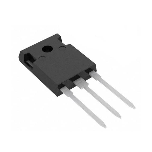
SPW17N80C3FKSA1 is listed in the Single FETs, MOSFETs range at ChipApex. The manufacturer field lists Infineon Technologies. Its product description is MOSFET N-CH 800V 17A TO247-3. Review the specifications below when checking this part for your BOM.
The SPW17N80C3FKSA1 is an N-Channel CoolMOS C3 power transistor in a PG-TO247-3 package. It features an 800 V drain-source breakdown voltage and a continuous drain current of 17 A at 25 °C case temperature. The device has a maximum on-state resistance of 0.29 Ω at 25 °C and a typical gate charge of 88 nC. Power dissipation reaches 227 W at 25 °C, with an operating junction temperature range from -55 °C to +150 °C.
Verify the specific ordering suffix FKSA1 against official Infineon documentation to confirm lead-free plating and packaging details. Confirm component lifecycle status as NRND (Not Recommended for New Designs) before initiating procurement. Ensure design reviews account for thermal management requirements specified in the datasheet.
Select this component for designs requiring robust high-voltage switching capabilities within the CoolMOS C3 family. Evaluate thermal resistance parameters to ensure adequate heat sinking for the specified power dissipation. Consider the gate charge characteristics when designing drive circuits for optimal switching efficiency.
This part belongs to the Infineon CoolMOS C3 series, utilizing silicon technology for high-voltage power control. It is designed as a single N-Channel enhancement mode MOSFET. The product line focuses on reducing conduction and switching losses in industrial power conversion systems.
SPW17N80C3
The single pulse avalanche energy (E_AS) is rated at 670 mJ under conditions of I_D = 3.4 A and V_DD = 50 V.
Yes, but wave soldering is only allowed at the leads, specifically 1.6 mm from the case for a duration of 10 seconds.
Explore related parts through FETs, MOSFETs, Transistors, Discrete Semiconductor Products, all product categories.
 SPW17N80C3FKSA1

SPW17N80C3FKSA1 is listed in the Single FETs, MOSFETs range at ChipApex. The manufacturer field lists Infineon Technologies. Its product description is MOSFET N-CH 800V…
Read More
SPW17N80C3FKSA1 is listed in the Single FETs, MOSFETs range at ChipApex. The manufacturer field lists Infineon Technologies. Its product description is MOSFET N-CH 800V…
Read More
SPW17N80C3FKSA1 is listed in the Single FETs, MOSFETs range at ChipApex. The manufacturer field lists Infineon Technologies. Its product description is MOSFET N-CH 800V…
Read More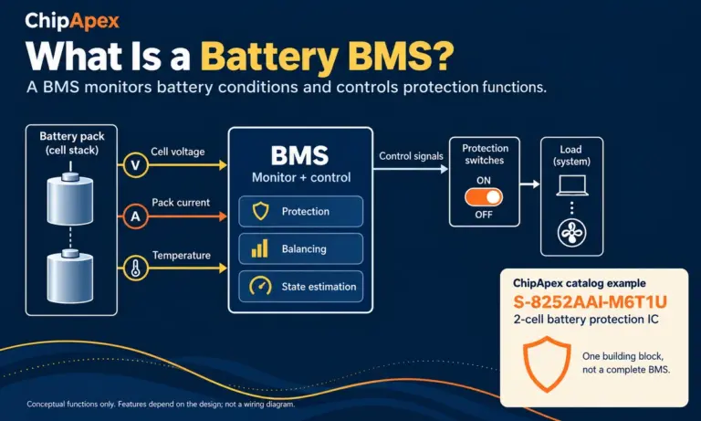
Learn what a battery BMS does, how protection differs from charging, and which pack specifications to check when sourcing BMS components through ChipApex.
Read More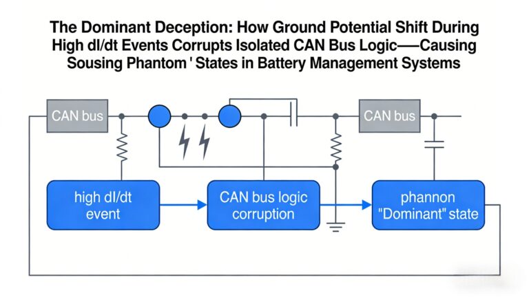
SPW17N80C3FKSA1 is listed in the Single FETs, MOSFETs range at ChipApex. The manufacturer field lists Infineon Technologies. Its product description is MOSFET N-CH 800V…
Read More
Find out when a bare shock switch needs a pull resistor, when an MCU internal pull-up is enough, and why sensor modules and piezo…
Read More
SPW17N80C3FKSA1 is listed in the Single FETs, MOSFETs range at ChipApex. The manufacturer field lists Infineon Technologies. Its product description is MOSFET N-CH 800V…
Read More
Learn how a diode conducts, how to identify anode and cathode, and when to choose rectifier, TVS, Zener or photodiode types for a circuit.
Read More
SPW17N80C3FKSA1 is listed in the Single FETs, MOSFETs range at ChipApex. The manufacturer field lists Infineon Technologies. Its product description is MOSFET N-CH 800V…
Read More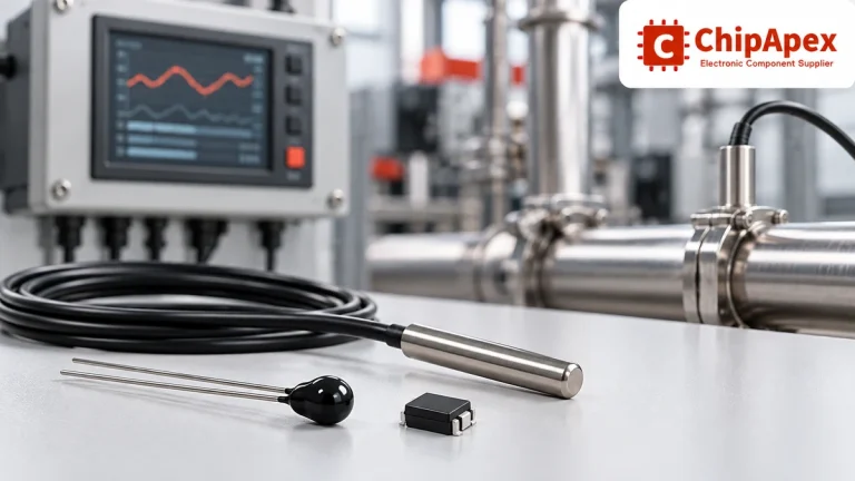
Compare thermistors, RTDs, thermocouples and temperature ICs. Learn how range, accuracy, response, interfaces and mounting affect component selection.
Read More
SPW17N80C3FKSA1 is listed in the Single FETs, MOSFETs range at ChipApex. The manufacturer field lists Infineon Technologies. Its product description is MOSFET N-CH 800V…
Read More
SPW17N80C3FKSA1 is listed in the Single FETs, MOSFETs range at ChipApex. The manufacturer field lists Infineon Technologies. Its product description is MOSFET N-CH 800V…
Read More
The activity of extra discounts on wholesale prices is in full swing…
Please fill in your contact information and we will send you the latest wholesale price list.