 ChipApex | Global Electronic Components Supplier

SEARCH
Search Product
Search Post
— IC芯片 | 连接器 | 传感器 | 被动器件 —
Search productSearch post
— IC芯片 | 连接器 | 传感器 | 被动器件 —
Consult the customer manager about the wholesale price.
consultation hotline:86-132-6715-2157
email:[email protected]
Contact the product manager for consultation. One-stop consultation is available.
Do you want a lower wholesale price? Please send us your inquiry and we will reply immediately.
TSM1285BCSA+T is listed in the Analog To Digital Converters (ADC) range at ChipApex. The manufacturer field lists Silicon Labs. Its product description is IC ADC 12BIT SAR 8SOIC. Review the specifications below when checking this part for your BOM.
The TSM1285BCSA+T is a single-supply, single-channel, 12-bit analog-to-digital converter (ADC) manufactured by Silicon Labs. It operates within a voltage range of +2.7V to +3.6V and features an internal +2.5V reference and track-and-hold circuit. The device supports a sampling rate of 300ksps with a full-power bandwidth of 3 MHz. Electrical specifications include ±1 LSB maximum DNL and INL, and a conversion time of 3.3 μs. It utilizes a 3-wire serial interface compatible with SPI, QSPI, and MICROWIRE standards. The component is housed in an 8-pin SOIC package and is specified for operation from 0°C to +70°C.
Verify the ordering suffix '+T' indicates tape and reel packaging containing 2500 units, distinct from the tube-packaged variant. Confirm the 'BC' suffix corresponds to the commercial temperature range of 0°C to +70°C. Ensure compatibility with existing PCB footprints for the 8-pin SOIC package. Check for end-of-life status or alternative sourcing requirements as this component may be discontinued.
Select the TSM1285BCSA+T when a 12-bit resolution and 300ksps speed are required for single-ended input signals. Choose this part over the BE variant if the application environment remains within the 0°C to +70°C range. Consider the internal 2.5V reference capability to reduce external component count. Ensure the system microcontroller supports the required 3-wire serial protocol up to 4.8MHz clock speeds.
The TSM1285 series serves as an alternate source for the Maxim Integrated MAX1285 and offers a higher-speed upgrade path compared to the MAX1240 and MAX1241 ADCs. The BC version specifically targets commercial applications, while the BE version covers industrial temperatures. Both share identical electrical characteristics but differ in operating temperature ranges and packaging quantities.
The TSM1285BCSA+T is functionally equivalent to the Maxim Integrated MAX1285BCSA+. Designers upgrading from MAX1240 or MAX1241 should verify pinout compatibility and interface timing differences. No other direct cross-model substitutes are documented in the provided datasheet.
The minimum acquisition time (tACQ) is 625 ns, calculated based on the internal switch resistance and input capacitance.
Driving the SHDN pin low shuts down the ADC, reducing the supply current to approximately 2μA. The internal reference is disabled during shutdown.
A 4.7μF capacitor is recommended between the REF pin and GND to maintain conversion accuracy within 1 LSB.
Explore related parts through Data Acquisition, Integrated Circuits (ICs), all product categories, ChipApex homepage.
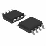 TSM1285BCSA+T

TSM1285BCSA+T is listed in the Analog To Digital Converters (ADC) range at ChipApex. The manufacturer field lists Silicon Labs. Its product description is IC…
Read More
TSM1285BCSA+T is listed in the Analog To Digital Converters (ADC) range at ChipApex. The manufacturer field lists Silicon Labs. Its product description is IC…
Read MoreTSM1285BCSA+T is listed in the Analog To Digital Converters (ADC) range at ChipApex. The manufacturer field lists Silicon Labs. Its product description is IC…
Read More
TSM1285BCSA+T is listed in the Analog To Digital Converters (ADC) range at ChipApex. The manufacturer field lists Silicon Labs. Its product description is IC…
Read More
TSM1285BCSA+T is listed in the Analog To Digital Converters (ADC) range at ChipApex. The manufacturer field lists Silicon Labs. Its product description is IC…
Read More
TSM1285BCSA+T is listed in the Analog To Digital Converters (ADC) range at ChipApex. The manufacturer field lists Silicon Labs. Its product description is IC…
Read More
Learn why PTC resistance rises with temperature, how it differs from NTC, and which ratings matter for sensing and protection.
Read More
Understand how a comparator switches at a voltage threshold, why hysteresis prevents chatter, and which output and input specs matter.
Read More
TSM1285BCSA+T is listed in the Analog To Digital Converters (ADC) range at ChipApex. The manufacturer field lists Silicon Labs. Its product description is IC…
Read More
TSM1285BCSA+T is listed in the Analog To Digital Converters (ADC) range at ChipApex. The manufacturer field lists Silicon Labs. Its product description is IC…
Read More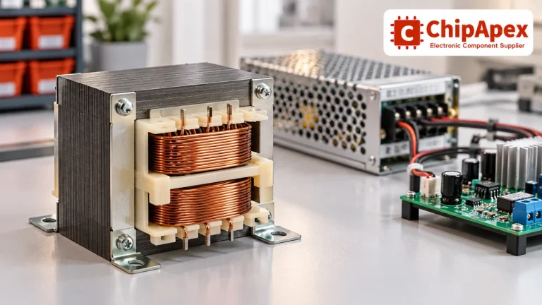
Select power transformers by input frequency, secondary VA, rectifier load, isolation, regulation and inrush. Build a clearer specification for your next RFQ.
Read More
TSM1285BCSA+T is listed in the Analog To Digital Converters (ADC) range at ChipApex. The manufacturer field lists Silicon Labs. Its product description is IC…
Read More
The activity of extra discounts on wholesale prices is in full swing…
Please fill in your contact information and we will send you the latest wholesale price list.





