 ChipApex | Global Electronic Components Supplier

SEARCH
Search Product
Search Post
— IC芯片 | 连接器 | 传感器 | 被动器件 —
Search productSearch post
— IC芯片 | 连接器 | 传感器 | 被动器件 —
Consult the customer manager about the wholesale price.
consultation hotline:86-132-6715-2157
email:[email protected]
Contact the product manager for consultation. One-stop consultation is available.
Do you want a lower wholesale price? Please send us your inquiry and we will reply immediately.
XC2V250-5FGG456I is listed in the Field Programmable Gate Array range at ChipApex. The manufacturer field lists AMD. Its product description is IC FPGA 200 I/O 456FBGA. Review the specifications below when checking this part for your BOM.
The XC2V250-5FGG456I is a Virtex-II Field Programmable Gate Array manufactured by Xilinx, now part of AMD. It utilizes a 0.15 µm CMOS process and operates with a 1.5 V core voltage (VCCINT). The device features 250K system gates, 1,536 slices within its Configurable Logic Blocks (CLBs), and supports up to 200 user I/Os in the FG456 package. Key architectural resources include 24 dedicated 18-bit x 18-bit multiplier blocks and 432 Kb of Block SelectRAM memory. It incorporates eight Digital Clock Manager (DCM) modules for clock synthesis and distribution.
Verify component authenticity through authorized distributors or direct manufacturer channels. Confirm that the ordering suffix 'GG' indicates Pb-free wire-bond packaging as specified in official documentation. Ensure compliance with RoHS directives if lead-free construction is required for the specific application environment.
Select this model when designs require 250K system gates with a 1.00 mm pitch fine-pitch BGA footprint. Consider the FGG456 package variant specifically for Pb-free manufacturing requirements. Evaluate the 200 available user I/Os against interface needs, noting that flip-chip packages offer higher pin counts for equivalent gate densities.
This component belongs to the Virtex-II family, representing an early platform FPGA solution optimized for high performance. It bridges low-density and high-density design capabilities using IP cores. The architecture introduced significant enhancements in routing predictability and embedded memory density compared to preceding generations.
Publicly confirmed substitute part numbers are not available in the provided source material. Designers should consult official migration guides for subsequent families such as Spartan-3 or Virtex-4/5 for functional equivalents.
The 'GG' suffix denotes a Pb-free wire-bond Fine-Pitch Ball Grid Array (BGA) package with a 1.00 mm pitch.
The XC2V250 device includes eight DCM blocks for clock distribution and management.
In the FG456 package, the device supports a maximum of 200 user I/O pads.
Explore related parts through Embedded, Integrated Circuits (ICs), all product categories, ChipApex homepage.
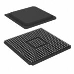 XC2V250-5FGG456I

Select MOV varistors by continuous voltage, clamping behavior, surge waveform and repetition. Check thermal disconnection, fuse coordination and replacements.
Read More
XC2V250-5FGG456I is listed in the Field Programmable Gate Array range at ChipApex. The manufacturer field lists AMD. Its product description is IC FPGA 200…
Read More
Select a bridge rectifier by reverse voltage, capacitor charging current, startup surge and cooling. Work through a stated DC voltage and ripple example.
Read More
XC2V250-5FGG456I is listed in the Field Programmable Gate Array range at ChipApex. The manufacturer field lists AMD. Its product description is IC FPGA 200…
Read More
XC2V250-5FGG456I is listed in the Field Programmable Gate Array range at ChipApex. The manufacturer field lists AMD. Its product description is IC FPGA 200…
Read More
XC2V250-5FGG456I is listed in the Field Programmable Gate Array range at ChipApex. The manufacturer field lists AMD. Its product description is IC FPGA 200…
Read More
XC2V250-5FGG456I is listed in the Field Programmable Gate Array range at ChipApex. The manufacturer field lists AMD. Its product description is IC FPGA 200…
Read More
XC2V250-5FGG456I is listed in the Field Programmable Gate Array range at ChipApex. The manufacturer field lists AMD. Its product description is IC FPGA 200…
Read More
Compare Pt100 and Pt1000 RTDs, two-, three- and four-wire connections, excitation and self-heating. Build an error budget from element to reported temperature.
Read More
XC2V250-5FGG456I is listed in the Field Programmable Gate Array range at ChipApex. The manufacturer field lists AMD. Its product description is IC FPGA 200…
Read More
XC2V250-5FGG456I is listed in the Field Programmable Gate Array range at ChipApex. The manufacturer field lists AMD. Its product description is IC FPGA 200…
Read More
XC2V250-5FGG456I is listed in the Field Programmable Gate Array range at ChipApex. The manufacturer field lists AMD. Its product description is IC FPGA 200…
Read More
The activity of extra discounts on wholesale prices is in full swing…
Please fill in your contact information and we will send you the latest wholesale price list.





