 ChipApex | Global Electronic Components Supplier

SEARCH
Search Product
Search Post
— IC芯片 | 连接器 | 传感器 | 被动器件 —
Search productSearch post
— IC芯片 | 连接器 | 传感器 | 被动器件 —
Consult the customer manager about the wholesale price.
consultation hotline:86-132-6715-2157
email:[email protected]
Contact the product manager for consultation. One-stop consultation is available.
Do you want a lower wholesale price? Please send us your inquiry and we will reply immediately.
XC2V40-5CSG144I is listed in the Field Programmable Gate Array range at ChipApex. The manufacturer field lists AMD. Its product description is IC FPGA 88 I/O 144CSBGA. Review the specifications below when checking this part for your BOM.
The XC2V40-5CSG144I is a Virtex-II Field Programmable Gate Array manufactured by Xilinx, now part of AMD. It features an array size of 8 rows by 8 columns, providing 256 slices and approximately 40K system gates. The device includes 8 dedicated multiplier blocks and four Digital Clock Manager (DCM) modules for clock synthesis and distribution. It utilizes the CS144 wire-bond Chip-Scale Ball Grid Array package with a 0.80 mm pitch, offering up to 88 user I/O pads. Operating at speed grade -5, it supports a core voltage of 1.5 V and auxiliary voltages of 3.3 V.
Verify component authenticity against original manufacturer markings. Confirm package integrity and pin alignment prior to installation. Ensure static discharge precautions are observed during handling. Validate that the specific ordering suffix matches the required temperature range and lead-free specifications for the target application environment.
Select this model when designs require moderate logic density within a compact chip-scale footprint. The CS144 package limits available I/O count compared to larger BGA options. Verify that the -5 speed grade meets timing requirements for the intended clock frequencies. Consider thermal dissipation capabilities inherent to the wire-bond construction for the final board layout.
This component belongs to the Virtex-II family, representing early platform FPGA technology utilizing a 0.15 µm process. It serves as a foundational solution for embedded logic before the introduction of higher-density Spartan and Virtex-4 series devices. The architecture establishes baseline resource definitions for subsequent generations of programmable logic.
Direct pin-compatible replacements are not available due to architectural differences in newer families. Migration typically requires schematic redesign and PCB re-layout. Consult official cross-reference guides for functional equivalents with adjusted resource allocations.
The CS144 package supports a maximum of 88 user I/O pads.
The device contains four DCM modules for clock management.
The internal core voltage (VCCINT) is specified as 1.5 V.
Explore related parts through Embedded, Integrated Circuits (ICs), all product categories, ChipApex homepage.
 XC2V40-5CSG144I
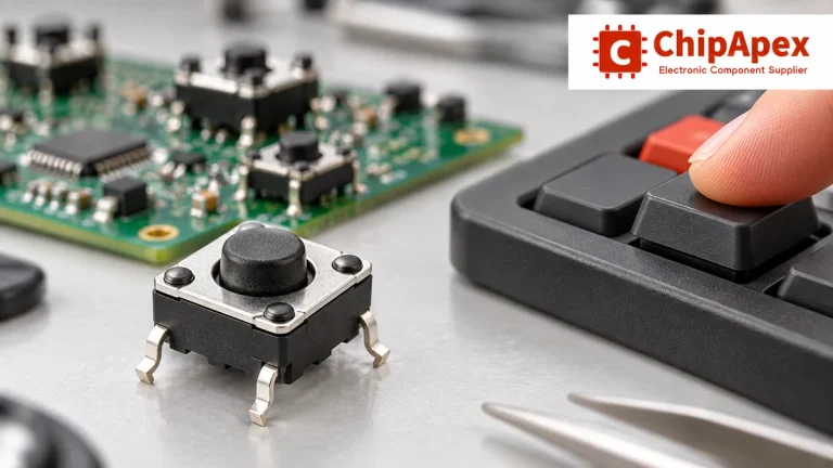
Understand tactile switches, PCB and keyboard differences, four-pin wiring, debounce, force, travel and replacement checks for reliable control inputs.
Read More
XC2V40-5CSG144I is listed in the Field Programmable Gate Array range at ChipApex. The manufacturer field lists AMD. Its product description is IC FPGA 88…
Read More
XC2V40-5CSG144I is listed in the Field Programmable Gate Array range at ChipApex. The manufacturer field lists AMD. Its product description is IC FPGA 88…
Read More
XC2V40-5CSG144I is listed in the Field Programmable Gate Array range at ChipApex. The manufacturer field lists AMD. Its product description is IC FPGA 88…
Read More
XC2V40-5CSG144I is listed in the Field Programmable Gate Array range at ChipApex. The manufacturer field lists AMD. Its product description is IC FPGA 88…
Read More
Find out when a bare shock switch needs a pull resistor, when an MCU internal pull-up is enough, and why sensor modules and piezo…
Read More
XC2V40-5CSG144I is listed in the Field Programmable Gate Array range at ChipApex. The manufacturer field lists AMD. Its product description is IC FPGA 88…
Read More
XC2V40-5CSG144I is listed in the Field Programmable Gate Array range at ChipApex. The manufacturer field lists AMD. Its product description is IC FPGA 88…
Read More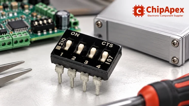
Choose a DIP switch by contact type, coded positions, footprint and signal ratings. Check logic polarity, assembly conditions and PCB configuration behavior.
Read More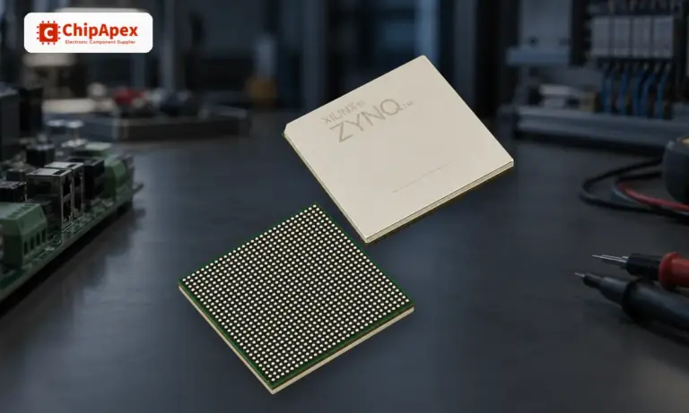
Learn what an integrated circuit is, how ICs work, the main types and the specs to check before choosing a part for your design…
Read More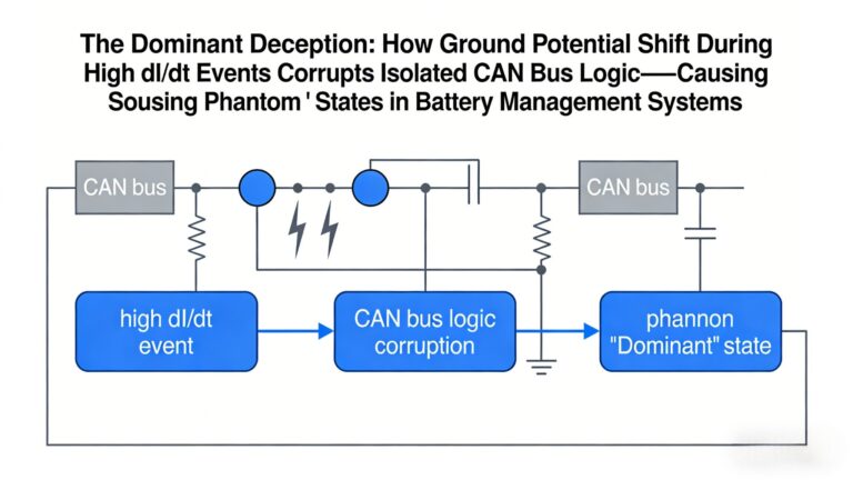
XC2V40-5CSG144I is listed in the Field Programmable Gate Array range at ChipApex. The manufacturer field lists AMD. Its product description is IC FPGA 88…
Read More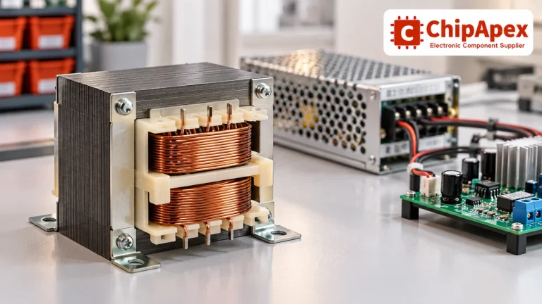
Select power transformers by input frequency, secondary VA, rectifier load, isolation, regulation and inrush. Build a clearer specification for your next RFQ.
Read More
The activity of extra discounts on wholesale prices is in full swing…
Please fill in your contact information and we will send you the latest wholesale price list.






