 ChipApex | Global Electronic Components Supplier

SEARCH
Search Product
Search Post
— IC芯片 | 连接器 | 传感器 | 被动器件 —
Search productSearch post
— IC芯片 | 连接器 | 传感器 | 被动器件 —
Consult the customer manager about the wholesale price.
consultation hotline:86-132-6715-2157
email:[email protected]
Contact the product manager for consultation. One-stop consultation is available.
Do you want a lower wholesale price? Please send us your inquiry and we will reply immediately.
XCV100E-7FG256C is listed in the Field Programmable Gate Array range at ChipApex. The manufacturer field lists AMD. Its product description is IC FPGA 176 I/O 256FBGA. Review the specifications below when checking this part for your BOM.
The XCV100E-7FG256C is a Virtex-E Field Programmable Gate Array manufactured by AMD (formerly Xilinx). It utilizes a 0.18 μm CMOS process with a 1.8 V core voltage and operates within the commercial temperature range of 0°C to +85°C. The device features 128,236 system gates, 32,400 logic gates, and 2,700 logic cells. It includes 81,920 bits of Block SelectRAM and 38,400 bits of distributed RAM. The FG256 package provides 176 user I/O pins. The -7 speed grade supports internal performance up to 130 MHz.
Verify the specific ordering suffix against official documentation to confirm the package type, speed grade, and industrial or commercial temperature rating. Ensure compatibility with the required design tools and development systems before procurement. Confirm that the pinout matches the intended PCB layout constraints.
Select this component when a balance of moderate logic density and high-speed performance is required. The 1.8 V core voltage offers lower power consumption compared to older 2.5 V families. Consider the FG256 package size relative to available board space and I/O requirements. Verify that the -7 speed grade meets the maximum clock frequency needs of the target application.
This part belongs to the Virtex-E family, which represents an evolutionary step from the original Virtex series. It offers higher performance and lower power due to the 0.18 μm process technology. While not bitstream-compatible with the original Virtex family, it maintains pin compatibility with some devices in the same package types.
XCV100E-6FG256C
No, the Virtex-E family is not bitstream-compatible with the original Virtex family. However, Virtex designs can be compiled into equivalent Virtex-E devices.
The internal logic and memory operate at a core voltage (VCCINT) of 1.8 V.
The XCV100E contains eight fully digital Delay-Locked Loops (DLLs).
Explore related parts through Embedded, Integrated Circuits (ICs), all product categories, ChipApex homepage.

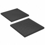 XCV100E-7FG256C
Choose logic inverter ICs by thresholds, supply, output drive and delay. Compare standard and Schmitt-trigger inputs, power sequencing and replacement checks.
Read More
Understand thermal fuse operation, Tf, Th and Tm, electrical ratings and mounting. Check temperature limits and replacement requirements for your design.
Read More
XCV100E-7FG256C is listed in the Field Programmable Gate Array range at ChipApex. The manufacturer field lists AMD. Its product description is IC FPGA 176…
Read More
Find out when a bare shock switch needs a pull resistor, when an MCU internal pull-up is enough, and why sensor modules and piezo…
Read More
XCV100E-7FG256C is listed in the Field Programmable Gate Array range at ChipApex. The manufacturer field lists AMD. Its product description is IC FPGA 176…
Read More
XCV100E-7FG256C is listed in the Field Programmable Gate Array range at ChipApex. The manufacturer field lists AMD. Its product description is IC FPGA 176…
Read More
XCV100E-7FG256C is listed in the Field Programmable Gate Array range at ChipApex. The manufacturer field lists AMD. Its product description is IC FPGA 176…
Read More
XCV100E-7FG256C is listed in the Field Programmable Gate Array range at ChipApex. The manufacturer field lists AMD. Its product description is IC FPGA 176…
Read More
XCV100E-7FG256C is listed in the Field Programmable Gate Array range at ChipApex. The manufacturer field lists AMD. Its product description is IC FPGA 176…
Read More
XCV100E-7FG256C is listed in the Field Programmable Gate Array range at ChipApex. The manufacturer field lists AMD. Its product description is IC FPGA 176…
Read More
XCV100E-7FG256C is listed in the Field Programmable Gate Array range at ChipApex. The manufacturer field lists AMD. Its product description is IC FPGA 176…
Read More
See how a MEMS gyroscope measures angular rate, why its angle estimate drifts, and which range, noise, interface and temperature specs to compare.
Read More
The activity of extra discounts on wholesale prices is in full swing…
Please fill in your contact information and we will send you the latest wholesale price list.



