 ChipApex | Global Electronic Components Supplier

SEARCH
Search Product
Search Post
— IC芯片 | 连接器 | 传感器 | 被动器件 —
Search productSearch post
— IC芯片 | 连接器 | 传感器 | 被动器件 —
Consult the customer manager about the wholesale price.
consultation hotline:86-132-6715-2157
email:[email protected]
Contact the product manager for consultation. One-stop consultation is available.
Do you want a lower wholesale price? Please send us your inquiry and we will reply immediately.
XCV600E-7BG560I is listed in the Field Programmable Gate Array range at ChipApex. The manufacturer field lists AMD. Its product description is IC FPGA 404 I/O 560MBGA. Review the specifications below when checking this part for your BOM.
The XCV600E-7BG560I is a Virtex-E Field Programmable Gate Array manufactured by Xilinx, utilizing a 0.18 μm CMOS process with 1.8 V core logic and 3.3 V I/O. It features 985,882 system gates, 186,624 logic gates, and 15,552 logic cells within a 48 x 72 CLB array. The device provides 294,912 bits of Block SelectRAM and 221,184 bits of distributed RAM. Operating at the -7 speed grade in a BG560 package, it supports up to 404 user I/Os.
Verify that the ordering suffix 'I' confirms the industrial temperature range (-40°C to +100°C). Confirm the '7' speed grade matches the required timing constraints for your design. Ensure the BG560 package dimensions align with your PCB footprint specifications before finalizing procurement.
Select this component when designs require approximately one million system gates with high-density block RAM resources. The Virtex-E family offers improved performance over standard Virtex devices while maintaining pin compatibility for many packages. Consider the -7 speed grade if synchronous system clock rates up to 240 MHz are sufficient for the application requirements.
This part belongs to the Virtex-E 1.8 V FPGA family, which represents an evolutionary step from the original Virtex series. It utilizes an advanced 0.18 μm six-layer metal process to achieve higher silicon efficiency and lower power consumption compared to previous generations. The family includes devices ranging from 58 k to 4 M system gates.
Virtex-E devices are not bitstream-compatible with the original Virtex family, though designs can be compiled into equivalent parts. For migration within the Virtex-E family, verify banking rules and VCCO/VREF configurations, as input buffers for LVTTL and LVCMOS standards are powered by VCCO rather than VCCINT.
Explore related parts through Embedded, Integrated Circuits (ICs), all product categories, ChipApex homepage.
 XCV600E-7BG560I

XCV600E-7BG560I is listed in the Field Programmable Gate Array range at ChipApex. The manufacturer field lists AMD. Its product description is IC FPGA 404…
Read More
XCV600E-7BG560I is listed in the Field Programmable Gate Array range at ChipApex. The manufacturer field lists AMD. Its product description is IC FPGA 404…
Read More
XCV600E-7BG560I is listed in the Field Programmable Gate Array range at ChipApex. The manufacturer field lists AMD. Its product description is IC FPGA 404…
Read More
XCV600E-7BG560I is listed in the Field Programmable Gate Array range at ChipApex. The manufacturer field lists AMD. Its product description is IC FPGA 404…
Read More
Learn the relay definition, coil and contact operation, NO and NC forms, load ratings and suppression choices. Compare mechanical, reed and solid-state types.
Read More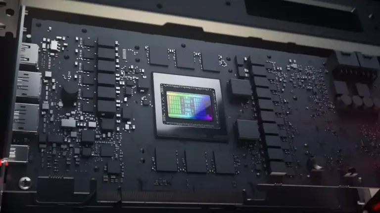
XCV600E-7BG560I is listed in the Field Programmable Gate Array range at ChipApex. The manufacturer field lists AMD. Its product description is IC FPGA 404…
Read More
XCV600E-7BG560I is listed in the Field Programmable Gate Array range at ChipApex. The manufacturer field lists AMD. Its product description is IC FPGA 404…
Read More
Learn what an IMU measures, how accelerometers and gyroscopes work together, why orientation estimates drift, and what to compare.
Read More
XCV600E-7BG560I is listed in the Field Programmable Gate Array range at ChipApex. The manufacturer field lists AMD. Its product description is IC FPGA 404…
Read More
XCV600E-7BG560I is listed in the Field Programmable Gate Array range at ChipApex. The manufacturer field lists AMD. Its product description is IC FPGA 404…
Read More
Find out when a bare shock switch needs a pull resistor, when an MCU internal pull-up is enough, and why sensor modules and piezo…
Read More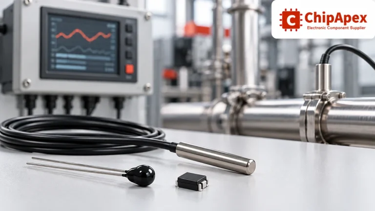
Compare thermistors, RTDs, thermocouples and temperature ICs. Learn how range, accuracy, response, interfaces and mounting affect component selection.
Read More
The activity of extra discounts on wholesale prices is in full swing…
Please fill in your contact information and we will send you the latest wholesale price list.






