 ChipApex | Global Electronic Components Supplier

SEARCH
Search Product
Search Post
— IC芯片 | 连接器 | 传感器 | 被动器件 —
Search productSearch post
— IC芯片 | 连接器 | 传感器 | 被动器件 —
The trend of science and technology is changing rapidly.
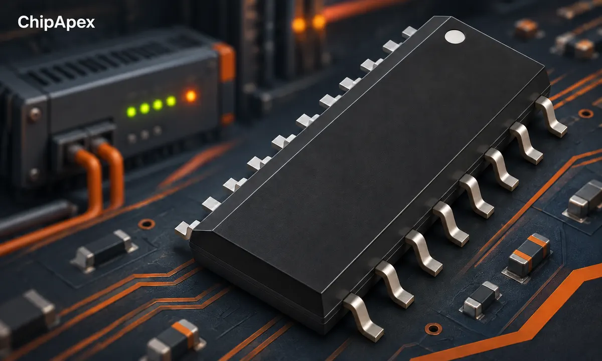
A shift register is a chain of storage elements that moves binary data one position on each active clock edge. It can convert serial data to parallel outputs, collect parallel inputs into a serial stream, or delay data by a known number of clock cycles.
A shift register is useful when a controller has limited input or output pins. The required data direction, output behavior and logic voltage determine the device type. The familiar eight-bit serial-to-parallel device is one example, not the definition of the whole category.
Each stage stores a bit. At the specified clock edge, a stage captures the value from the preceding stage while the first stage captures the serial input. The timing rules ensure that the old values move through the chain predictably.
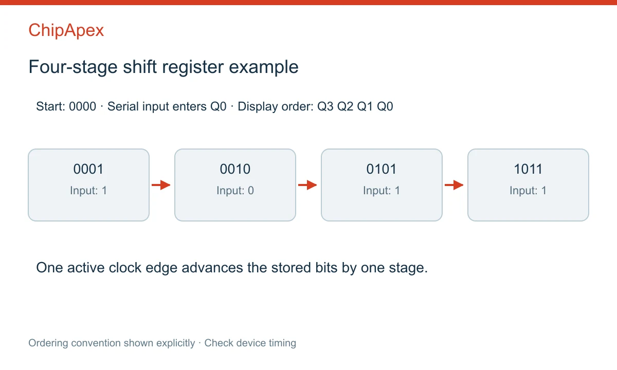
Consider a four-stage example labeled Q0 through Q3, with data entering Q0. Starting at 0000, serial inputs 1, 0, 1, 1 produce these states when listed as Q3 Q2 Q1 Q0: 0001, 0010, 0101, 1011. The ordering convention matters. A diagram that lists Q0 first will display the same stored bits differently.
The device's datasheet specifies whether shifting occurs on a rising or falling edge. It also defines setup and hold time: data must be stable for a required interval around that edge. Software that changes data and clock too close together can violate these limits even at a modest average update rate.
| Type | Data enters | Data leaves | Typical purpose |
|---|---|---|---|
| SIPO | Serially | In parallel | Expand controller outputs |
| PISO | In parallel | Serially | Read switches or digital inputs |
| SISO | Serially | Serially | Delay or pipeline a bit stream |
| PIPO | In parallel | In parallel | Store or transfer a parallel word |
PIPO operation describes parallel register behavior; a basic PIPO register need not shift. Universal shift registers can support several modes, sometimes including shift-left, shift-right and parallel load. Check the mode table instead of assuming all register ICs have the same controls.
Input expansion and output expansion also require different wiring and software sequences. A PISO part may need a parallel-load pulse before shifting out the captured input state. A SIPO part may need a separate latch pulse before new data appears at its outputs.
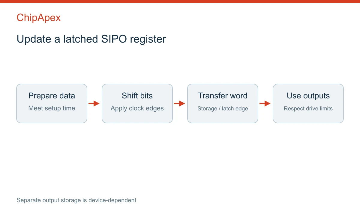
Some serial-to-parallel devices contain both a shift register and a separate storage register. Bits move through the shift stages while the output storage retains the previous word. A latch or storage-clock event then transfers the completed word to the outputs together.
Without that separation, intermediate shifting states may appear at the outputs. That can be acceptable in one circuit and disruptive in another. Indicator patterns, relay control and multiplexed selection signals often need deliberate update behavior.
The manufacturer's shift register overview distinguishes loading and storage options. The I/O expansion application note provides further design context for daisy-chained registers.
Output enable and reset also serve different functions. An output-enable input may place pins in a high-impedance state without clearing stored data. A reset may clear only the shift stages, leaving a separate output storage register unchanged until another control event. Read the truth table for the specific device.
Connecting the serial output of one device to the serial input of the next extends the chain. Clock and control lines can often be shared, subject to loading and timing limits. The first word shifted may end up in the device farthest from the controller, depending on the wiring and bit order.
For three eight-bit devices, one complete update requires 24 shifted bits. At a 1 MHz clock, the ideal shifting time is 24 microseconds, before software overhead and latch timing. This calculation says nothing about whether 1 MHz meets the chosen parts' setup, hold and propagation requirements.
Long wiring, high fanout and fast edges can cause ringing or skew. A clock frequency well below the datasheet maximum does not guarantee clean signals on a poorly routed board. Check the waveform at the receiving device and provide local supply decoupling.
Match the input-high and input-low thresholds to the controller's actual output voltages. A nominal 3.3 V controller is not automatically compatible with every register powered at 5 V. Supply range, input tolerance and logic family must be evaluated together.
Output current limits apply per pin and often to the whole package. An absolute maximum is not a recommended operating point. LED loads need suitable current limiting, and inductive or high-current loads generally need a driver stage and appropriate protection. A logic register should not be treated as a relay driver without checking those requirements.
For boards that control relays, define the safe startup state before enabling outputs. For a removable interface, specify the connector header pinout so that data, clock, control and ground cannot be confused during assembly.
Send ChipApex the desired input/output mode, bit count, supply, clock rate, output-drive requirement, package and quantity. Include the preferred part number when replacing an existing design. A footprint match does not prove matching control polarity or startup behavior.
No. A shift register moves data through a defined sequence of stages. RAM provides addressed storage with a different access model.
No. Some have a separate output storage register, while others expose the shifting stages or provide different operating modes.
Often, a controller's SPI hardware can generate compatible serial data and clock signals. You still need to check edge timing, bit order and any separate load or latch control.
The software bit order, chain order or output-label convention may differ from the assumed mapping. Test a single moving bit and compare it with the actual pinout.
A general logic register usually cannot. Use a suitable power driver and verify startup, protection and current requirements for the motor circuit.
Compare Hall, shunt, current transformer and Rogowski sensing. Check AC/DC capability, accuracy, isolation, heat and response before selecting a sensor.
View details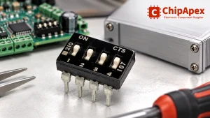
Choose a DIP switch by contact type, coded positions, footprint and signal ratings. Check logic polarity, assembly conditions and PCB configuration behavior.
View details
Discover how NOR flash enables fast code execution in embedded systems, its key types (Parallel/SPI), and how to source authentic, traceable ICs from trusted suppliers.
View details
Choose an ADC converter by resolution, sample rate, noise and input design. Review practical tradeoffs and prepare component requirements for ChipApex.
View details
The activity of extra discounts on wholesale prices is in full swing…
Please fill in your contact information and we will send you the latest wholesale price list.

