 ChipApex | Global Electronic Components Supplier

SEARCH
Search Product
Search Post
— IC芯片 | 连接器 | 传感器 | 被动器件 —
Search productSearch post
— IC芯片 | 连接器 | 传感器 | 被动器件 —
The trend of science and technology is changing rapidly.
A logic gate reads binary inputs and applies a rule to produce one output. AND requires every input to be high. OR requires at least one. A two-input XOR flags a mismatch. On a board, the gate also needs to recognize the incoming voltage levels and respond before its output is sampled.
Start with the truth table. It tells you what the output should do for every input combination, even when a schematic uses a symbol you don’t recognize. The table below covers six two-input gates. The inverter has only one input, so its rule is simpler: 0 becomes 1, and 1 becomes 0.
| A B | AND | OR | NAND | NOR | XOR | XNOR |
|---|---|---|---|---|---|---|
| 0 0 | 0 | 0 | 1 | 1 | 0 | 1 |
| 0 1 | 0 | 1 | 1 | 0 | 1 | 0 |
| 1 0 | 0 | 1 | 1 | 0 | 1 | 0 |
| 1 1 | 1 | 1 | 0 | 0 | 0 | 1 |
An output bubble on a schematic indicates inversion. Add one to an AND symbol and the result is NAND. An XOR symbol resembles an OR symbol with an extra curved line on the input side in common distinctive-shape notation. The logic gate reference shows the connection between symbols and output rules.
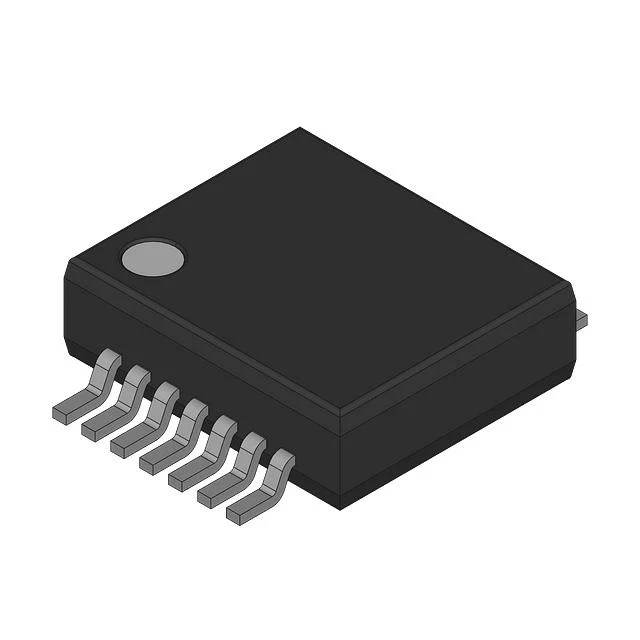
A gate that drives an active-high enable must produce a high output when the desired input conditions are true. Read the signal label and any inversion bubbles before connecting the output.
NAND gates are universal. Tie the inputs of one NAND together to invert a signal, or combine several NAND gates to build another Boolean function. In a board design, the right gate count also depends on delay, routing and what is already available in the package.
A NAND gate can invert a signal when its inputs are tied together. You can also combine NAND gates to build other Boolean functions. In a board design, compare package count and added stage delay before choosing that approach.
Slow or noisy inputs deserve a separate check. A Schmitt-trigger input has distinct rising and falling thresholds, which can help with slow transitions. The SN74HCS00 datasheet shows how one part specifies those thresholds as well as propagation delay. For a new design, also check power sequencing, input tolerance, capacitive load and the recommended state for any unused inputs. For an inverter gate IC, compare thresholds and package options. The logic inverter guide explains the single-input case in more detail.
Two chips can agree on a truth table and disagree on what counts as high. Consider a hypothetical driver whose data sheet guarantees at least 2.9 V high and at most 0.4 V low at the planned load. A receiver requiring at least 3.5 V high and accepting at most 1.5 V low gives a high-state margin of 2.9 − 3.5 = −0.6 V and a low-state margin of 1.5 − 0.4 = +1.1 V. The low level is within specification. The high level needs a compatible receiver or a level translator. These are example values, not ratings for an individual part.
On a board that combines POWER_GOOD and ENABLE, check whether the receiving pin is active low before choosing AND or NAND. If the inputs are asynchronous, unequal path delays can also create a short pulse. Check the timing at the receiving pin, especially if the receiver reacts to edges. For a slowly changing source, check the receiver’s maximum input transition time or choose a suitable Schmitt-trigger gate.
A half adder is a useful way to check the truth table on a breadboard. Feed both inputs to XOR and AND. XOR gives the sum bit, while AND gives the carry. At A = B = 1, the outputs are carry 1 and sum 0, which read as binary 10.
They implement decisions in hardware. A few gates can combine status flags or decode a control signal. Larger combinations implement arithmetic and data routing. A simple combinational gate responds to its inputs after a propagation delay. Circuits that retain state use storage elements or feedback.
Two paths reaching a gate can have different propagation delays, so the input combination can briefly pass through another state. Check the output with an oscilloscope and consider whether the receiving circuit samples the signal during that interval.
Follow the datasheet’s termination guidance. A floating CMOS input can settle near its threshold, respond to coupled noise, or increase current consumption. Connect unused inputs to defined states as recommended for the device and function.
The bubble shows inversion at the terminal. Active-low naming describes the logic level at which a function is asserted. Read both the symbol and the signal labels when you work through a schematic.
For two inputs, XOR goes high when the bits differ. XNOR goes high when the bits match. For example, both bits high gives XOR = 0 and XNOR = 1.
For a ChipApex quote, share the required gate function, logic family, supply voltage, package and target quantity.

Discover what DRAM is, how it works, its types, and why choosing authentic, RoHS-compliant DRAM chips matters. Source reliable DRAM from ChipApex—global supplier with full traceability.
View details
Compare screw and spring terminal blocks. Check conductor range, ferrules, strip length, torque, pitch and DIN rail accessories before completing the BOM.
View details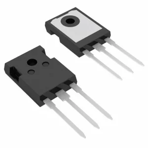
Learn how an IGBT works, compare MOSFET and IGBT losses, and check switching energy, gate drive, thermal limits and protection using a worked example.
View details
An inductor is approximately linear only over a specified operating range. In the ideal model, its inductance stays constant and voltage equals inductance times the rate of current change. A real magnetic core can approach saturation as current ri...
View details
The activity of extra discounts on wholesale prices is in full swing…
Please fill in your contact information and we will send you the latest wholesale price list.