 ChipApex | Global Electronic Components Supplier

SEARCH
Search Product
Search Post
— IC芯片 | 连接器 | 传感器 | 被动器件 —
Search productSearch post
— IC芯片 | 连接器 | 传感器 | 被动器件 —
Consult the customer manager about the wholesale price.
consultation hotline:86-132-6715-2157
email:[email protected]
Contact the product manager for consultation. One-stop consultation is available.
Do you want a lower wholesale price? Please send us your inquiry and we will reply immediately.
25AA040-I/P is listed in the Memory IC range at ChipApex. The manufacturer field lists Microchip Technology. Its product description is IC EEPROM 4KBIT SPI 1MHZ 8DIP. Review the specifications below when checking this part for your BOM.
The Microchip Technology 25AA040-I/P is a 4 Kbit (512 x 8-bit) serial Electrically Erasable PROM. It operates within a supply voltage range of 1.8V to 5.5V and supports a maximum clock frequency of 1 MHz. The device utilizes an SPI-compatible interface with separate data in (SI) and data out (SO) lines, synchronized by a clock input (SCK). Access is controlled via a Chip Select (CS) input, and communication can be paused using the HOLD pin. The component features block write protection, self-timed erase/write cycles, and high reliability with over 1 million endurance cycles and greater than 200 years of data retention.
Verify that the specific ordering suffix matches the required package type, as the 'P' designation indicates an 8-lead Plastic Dual In-line Package. Confirm the temperature grade corresponds to industrial specifications (-40°C to +85°C). Ensure the design accounts for the device being marked as not recommended for new designs, suggesting evaluation of newer alternatives like the 25AA040A series if applicable.
Select this component when a wide supply voltage range from 1.8V to 5.5V is required for compatibility with various logic levels. The 1 MHz clock speed suits applications where moderate data transfer rates are sufficient. Consider the 8-pin PDIP package for through-hole prototyping or legacy board designs. Evaluate the need for the HOLD pin functionality if bus sharing with other peripherals is necessary.
This part belongs to the 25XX040 family, which includes variants like the 25LC040 and 25C040. These devices share similar functional architectures but differ in operating voltage ranges and maximum clock frequencies. The 25AA040 specifically targets applications requiring operation down to 1.8V, distinguishing it from the 2.5V minimum 25LC040 and the 4.5V minimum 25C040.
Public confirmed substitute part numbers: 25AA040A-I/P
The HOLD pin allows the host to pause transmission without resetting the sequence. When pulled low while SCK is low, the SI, SCK, and SO pins enter a high-impedance state. Communication resumes when HOLD is brought high while SCK is low.
Upon power-up, the device enters low-power Standby mode, and the write enable latch is automatically reset. A WREN instruction must be issued before any write operations can be completed.
Explore related parts through Memory, Integrated Circuits (ICs), all product categories, ChipApex homepage.
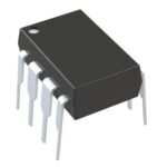 25AA040-I/P
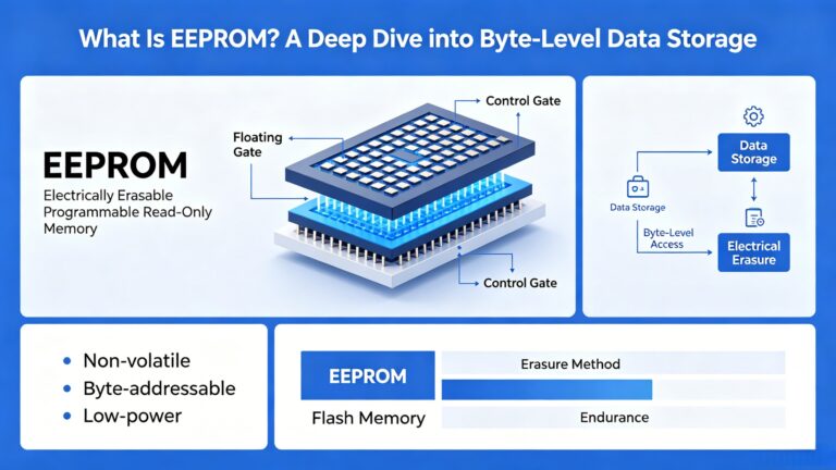
25AA040-I/P is listed in the Memory IC range at ChipApex. The manufacturer field lists Microchip Technology. Its product description is IC EEPROM 4KBIT SPI…
Read More
25AA040-I/P is listed in the Memory IC range at ChipApex. The manufacturer field lists Microchip Technology. Its product description is IC EEPROM 4KBIT SPI…
Read More
25AA040-I/P is listed in the Memory IC range at ChipApex. The manufacturer field lists Microchip Technology. Its product description is IC EEPROM 4KBIT SPI…
Read More
Find out when a bare shock switch needs a pull resistor, when an MCU internal pull-up is enough, and why sensor modules and piezo…
Read More
Understand UART protocol framing, baud rate and electrical interfaces. Learn 8N1 timing, TX/RX wiring, buffering and practical troubleshooting steps.
Read More
25AA040-I/P is listed in the Memory IC range at ChipApex. The manufacturer field lists Microchip Technology. Its product description is IC EEPROM 4KBIT SPI…
Read More
Learn what data acquisition means, from sensors and conditioning to sampling and storage. Review channel timing, wiring, calibration and data quality.
Read More
Learn how a pressure transducer converts pressure into voltage, current, or digital output, and compare pressure references and key selection specs.
Read More
25AA040-I/P is listed in the Memory IC range at ChipApex. The manufacturer field lists Microchip Technology. Its product description is IC EEPROM 4KBIT SPI…
Read More
25AA040-I/P is listed in the Memory IC range at ChipApex. The manufacturer field lists Microchip Technology. Its product description is IC EEPROM 4KBIT SPI…
Read More
25AA040-I/P is listed in the Memory IC range at ChipApex. The manufacturer field lists Microchip Technology. Its product description is IC EEPROM 4KBIT SPI…
Read More
25AA040-I/P is listed in the Memory IC range at ChipApex. The manufacturer field lists Microchip Technology. Its product description is IC EEPROM 4KBIT SPI…
Read More
The activity of extra discounts on wholesale prices is in full swing…
Please fill in your contact information and we will send you the latest wholesale price list.





