 ChipApex | Global Electronic Components Supplier

SEARCH
Search Product
Search Post
— IC芯片 | 连接器 | 传感器 | 被动器件 —
Search productSearch post
— IC芯片 | 连接器 | 传感器 | 被动器件 —
Consult the customer manager about the wholesale price.
consultation hotline:86-132-6715-2157
email:[email protected]
Contact the product manager for consultation. One-stop consultation is available.
Do you want a lower wholesale price? Please send us your inquiry and we will reply immediately.
5SGXMA7K2F40C3WN is listed in the Field Programmable Gate Array range at ChipApex. The manufacturer field lists Altera. Its product description is IC FPGA 696 I/O 1517FBGA. Review the specifications below when checking this part for your BOM.
The Altera 5SGXMA7K2F40C3WN is a Stratix V GX Field Programmable Gate Array featuring 622,000 logic elements and 234,720 adaptive logic modules. It includes 50 Mbit of embedded memory and supports 696 I/Os within a 1517-ball FCBGA package. The device operates at data rates up to 14.1 Gb/s with 36 transceivers. Core voltage ranges from 0.82V to 0.88V, with an operating temperature range of 0°C to 85°C.
Verify component authenticity and physical condition upon receipt, as this part may be discontinued or subject to supply chain limitations. Confirm that the specific suffix matches your design requirements exactly. Ensure proper handling procedures are followed due to moisture sensitivity classification. Validate compatibility with existing PCB layouts and thermal management solutions before final integration into production systems.
Select this model when requiring high-density logic combined with substantial embedded memory in a single FPGA solution. Consider the 1517-ball package constraints and pin availability during schematic capture. Evaluate power consumption profiles against available cooling capabilities. Ensure design tools support the specific Stratix V architecture features required for implementation.
This component belongs to the Stratix V GX family, designed for high-speed serial communication applications. It shares architectural similarities with other devices in the series but offers distinct resource counts. The part number indicates specific performance grades and packaging options tailored for demanding industrial and commercial environments requiring robust programmable logic capabilities.
Direct substitutes include the 5SGXMA7K3F40I3N and 5SGXEA7K3F40C3G. Verify pinout compatibility and resource adequacy before substitution. Cross-reference datasheets to ensure functional equivalence regarding transceiver specifications and memory configurations for seamless design migration.
Explore related parts through Embedded, Integrated Circuits (ICs), all product categories, ChipApex homepage.


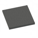 5SGXMA7K2F40C3WN

5SGXMA7K2F40C3WN is listed in the Field Programmable Gate Array range at ChipApex. The manufacturer field lists Altera. Its product description is IC FPGA 696…
Read More
5SGXMA7K2F40C3WN is listed in the Field Programmable Gate Array range at ChipApex. The manufacturer field lists Altera. Its product description is IC FPGA 696…
Read More
5SGXMA7K2F40C3WN is listed in the Field Programmable Gate Array range at ChipApex. The manufacturer field lists Altera. Its product description is IC FPGA 696…
Read More
5SGXMA7K2F40C3WN is listed in the Field Programmable Gate Array range at ChipApex. The manufacturer field lists Altera. Its product description is IC FPGA 696…
Read More
5SGXMA7K2F40C3WN is listed in the Field Programmable Gate Array range at ChipApex. The manufacturer field lists Altera. Its product description is IC FPGA 696…
Read More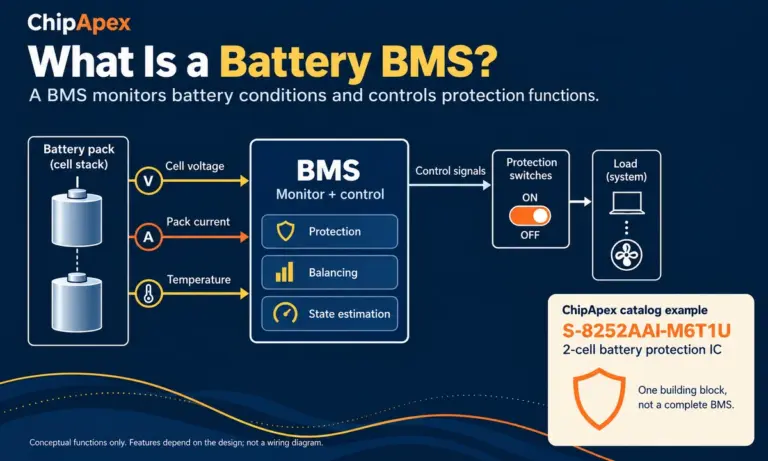
Learn what a battery BMS does, how protection differs from charging, and which pack specifications to check when sourcing BMS components through ChipApex.
Read More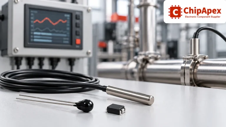
Compare thermistors, RTDs, thermocouples and temperature ICs. Learn how range, accuracy, response, interfaces and mounting affect component selection.
Read More
5SGXMA7K2F40C3WN is listed in the Field Programmable Gate Array range at ChipApex. The manufacturer field lists Altera. Its product description is IC FPGA 696…
Read More
5SGXMA7K2F40C3WN is listed in the Field Programmable Gate Array range at ChipApex. The manufacturer field lists Altera. Its product description is IC FPGA 696…
Read More
Select a bridge rectifier by reverse voltage, capacitor charging current, startup surge and cooling. Work through a stated DC voltage and ripple example.
Read More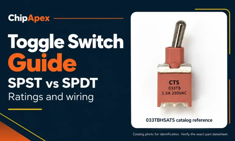
Compare SPST and SPDT toggle switches, understand AC/DC ratings, and follow wiring examples. Check contact action, mounting and parts in the ChipApex catalog.
Read More
See how a MEMS gyroscope measures angular rate, why its angle estimate drifts, and which range, noise, interface and temperature specs to compare.
Read More
The activity of extra discounts on wholesale prices is in full swing…
Please fill in your contact information and we will send you the latest wholesale price list.



