 ChipApex | Global Electronic Components Supplier

SEARCH
Search Product
Search Post
— IC芯片 | 连接器 | 传感器 | 被动器件 —
Search productSearch post
— IC芯片 | 连接器 | 传感器 | 被动器件 —
Consult the customer manager about the wholesale price.
consultation hotline:86-132-6715-2157
email:[email protected]
Contact the product manager for consultation. One-stop consultation is available.
Do you want a lower wholesale price? Please send us your inquiry and we will reply immediately.
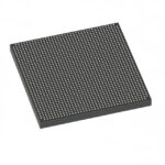
5SGXMA7N3F40C2LN is listed in the Field Programmable Gate Array range at ChipApex. The manufacturer field lists Altera. Its product description is IC FPGA 600 I/O 1517FBGA. Review the specifications below when checking this part for your BOM.
The Altera 5SGXMA7N3F40C2LN is a Stratix V GX Field Programmable Gate Array (FPGA) designed for high-performance digital signal processing and networking applications. It features 622,000 logic elements and 234,720 Adaptive Logic Modules (ALMs). The device integrates 50 Mbit of embedded memory and supports up to 14.1 Gb/s data rates across its transceivers. It operates within a commercial temperature range of 0°C to +70°C with a core voltage of 850 mV. The component is housed in a 1517-ball FBGA package suitable for surface mount technology.
Verify the specific suffix codes against official manufacturer documentation to confirm pinout compatibility and electrical specifications. Confirm end-of-life status or obsolescence notices prior to procurement planning. Ensure that any substitute components maintain identical thermal and mechanical constraints for the target application environment.
Select this model when the design requires a balance of moderate logic density and high-speed serial connectivity within the Stratix V family. Evaluate power consumption profiles at the target operating frequency to ensure adequate thermal management solutions are implemented on the printed circuit board layout.
This component belongs to the Stratix V GX series, which targets gigabit networking and DSP-intensive applications. It shares architectural similarities with other devices in the 5SGXMA7 family but differs in I/O count and package configuration. The GX designation indicates optimized transceiver performance for serial communication standards.
Publicly confirmed direct substitutes are not available in the provided source material. Consider reviewing the broader Stratix V FPGA portfolio for alternative packages or I/O configurations if exact pin-to-pin compatibility is required.
Explore related parts through Embedded, Integrated Circuits (ICs), all product categories, ChipApex homepage.
 5SGXMA7N3F40C2LN

5SGXMA7N3F40C2LN is listed in the Field Programmable Gate Array range at ChipApex. The manufacturer field lists Altera. Its product description is IC FPGA 600…
Read More
5SGXMA7N3F40C2LN is listed in the Field Programmable Gate Array range at ChipApex. The manufacturer field lists Altera. Its product description is IC FPGA 600…
Read More
5SGXMA7N3F40C2LN is listed in the Field Programmable Gate Array range at ChipApex. The manufacturer field lists Altera. Its product description is IC FPGA 600…
Read More
5SGXMA7N3F40C2LN is listed in the Field Programmable Gate Array range at ChipApex. The manufacturer field lists Altera. Its product description is IC FPGA 600…
Read More
5SGXMA7N3F40C2LN is listed in the Field Programmable Gate Array range at ChipApex. The manufacturer field lists Altera. Its product description is IC FPGA 600…
Read More
5SGXMA7N3F40C2LN is listed in the Field Programmable Gate Array range at ChipApex. The manufacturer field lists Altera. Its product description is IC FPGA 600…
Read More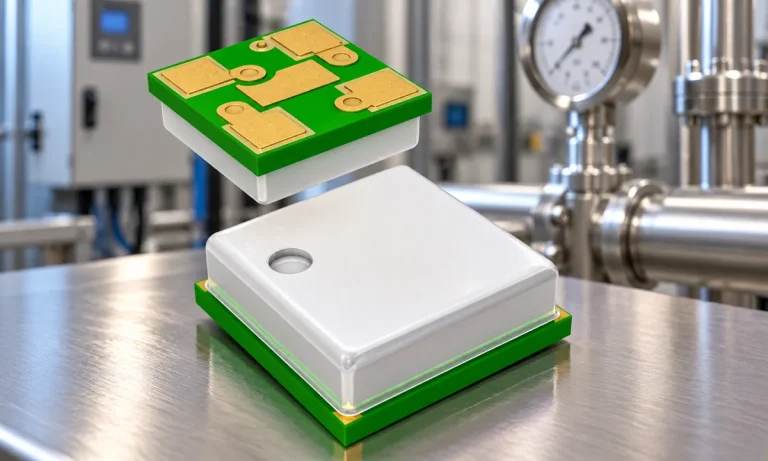
Learn how a pressure transducer converts pressure into voltage, current, or digital output, and compare pressure references and key selection specs.
Read More
See how a MEMS gyroscope measures angular rate, why its angle estimate drifts, and which range, noise, interface and temperature specs to compare.
Read More
5SGXMA7N3F40C2LN is listed in the Field Programmable Gate Array range at ChipApex. The manufacturer field lists Altera. Its product description is IC FPGA 600…
Read More
5SGXMA7N3F40C2LN is listed in the Field Programmable Gate Array range at ChipApex. The manufacturer field lists Altera. Its product description is IC FPGA 600…
Read More
Understand how a comparator switches at a voltage threshold, why hysteresis prevents chatter, and which output and input specs matter.
Read More
Select power transformers by input frequency, secondary VA, rectifier load, isolation, regulation and inrush. Build a clearer specification for your next RFQ.
Read More
The activity of extra discounts on wholesale prices is in full swing…
Please fill in your contact information and we will send you the latest wholesale price list.





