 ChipApex | Global Electronic Components Supplier

SEARCH
Search Product
Search Post
— IC芯片 | 连接器 | 传感器 | 被动器件 —
Search productSearch post
— IC芯片 | 连接器 | 传感器 | 被动器件 —
Consult the customer manager about the wholesale price.
consultation hotline:86-132-6715-2157
email:[email protected]
Contact the product manager for consultation. One-stop consultation is available.
Do you want a lower wholesale price? Please send us your inquiry and we will reply immediately.
74HC299D,652 is listed in the Shift Registers range at ChipApex. The manufacturer field lists Nexperia USA Inc.. Its product description is IC UNIV SHIFT REGISTER 20SOIC. Review the specifications below when checking this part for your BOM.
The Nexperia 74HC299D,652 is an 8-bit universal shift register with 3-state outputs housed in a SO20 (SOT163-1) package. It contains eight edge-triggered D-type flip-flops and interstage logic for synchronous shift-right, shift-left, parallel load, and hold operations. The I/O0 to I/O7 pins serve as multiplexed inputs/outputs. Supply voltage ranges from 2.0 V to 6.0 V. Propagation delay from CP to Q0/Q7 is typically 24 ns at 4.5 V. Maximum clock frequency is 45 MHz at 4.5 V.
Verify the specific ordering suffix against current Nexperia documentation to confirm package type and temperature range. Confirm availability status as manufacturing changes may occur. Ensure design compliance with absolute maximum ratings before integration.
Select this component when an 8-bit universal shift register with tri-state outputs is required. Verify that the supply voltage range of 2.0 V to 6.0 V matches the system requirements. Check propagation delay specifications against timing constraints for the target clock frequency.
This device belongs to the 74HC family of high-speed CMOS logic products manufactured by Nexperia. It provides standard logic functions compatible with various digital interfaces. The product data sheet defines its electrical characteristics, pin configurations, and functional behavior for design implementation.
Check for equivalent part numbers within the 74HC299 family or other manufacturers offering identical pinouts and logic functions. Verify compatibility with existing board layouts and signal integrity requirements before substitution.
Explore related parts through Logic, Integrated Circuits (ICs), all product categories, ChipApex homepage.
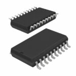 74HC299D,652
74HC299D,652 is listed in the Shift Registers range at ChipApex. The manufacturer field lists Nexperia USA Inc.. Its product description is IC UNIV SHIFT…
Read More
74HC299D,652 is listed in the Shift Registers range at ChipApex. The manufacturer field lists Nexperia USA Inc.. Its product description is IC UNIV SHIFT…
Read More
74HC299D,652 is listed in the Shift Registers range at ChipApex. The manufacturer field lists Nexperia USA Inc.. Its product description is IC UNIV SHIFT…
Read More
74HC299D,652 is listed in the Shift Registers range at ChipApex. The manufacturer field lists Nexperia USA Inc.. Its product description is IC UNIV SHIFT…
Read More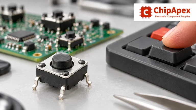
Understand tactile switches, PCB and keyboard differences, four-pin wiring, debounce, force, travel and replacement checks for reliable control inputs.
Read More
74HC299D,652 is listed in the Shift Registers range at ChipApex. The manufacturer field lists Nexperia USA Inc.. Its product description is IC UNIV SHIFT…
Read More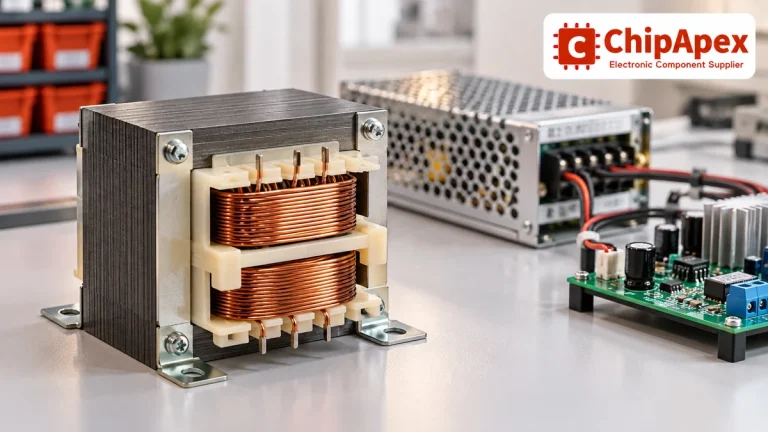
Select power transformers by input frequency, secondary VA, rectifier load, isolation, regulation and inrush. Build a clearer specification for your next RFQ.
Read More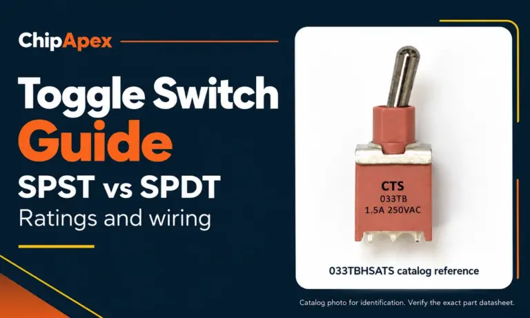
Compare SPST and SPDT toggle switches, understand AC/DC ratings, and follow wiring examples. Check contact action, mounting and parts in the ChipApex catalog.
Read More
74HC299D,652 is listed in the Shift Registers range at ChipApex. The manufacturer field lists Nexperia USA Inc.. Its product description is IC UNIV SHIFT…
Read More
74HC299D,652 is listed in the Shift Registers range at ChipApex. The manufacturer field lists Nexperia USA Inc.. Its product description is IC UNIV SHIFT…
Read More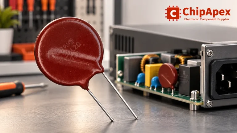
Select MOV varistors by continuous voltage, clamping behavior, surge waveform and repetition. Check thermal disconnection, fuse coordination and replacements.
Read More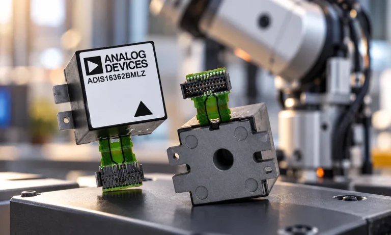
Learn what an IMU measures, how accelerometers and gyroscopes work together, why orientation estimates drift, and what to compare.
Read More
The activity of extra discounts on wholesale prices is in full swing…
Please fill in your contact information and we will send you the latest wholesale price list.






