ChipApex | Global Electronic Components Supplier
74LCX32245GX
Search Product
Search Post
— IC芯片 | 连接器 | 传感器 | 被动器件 —
Search productSearch post
— IC芯片 | 连接器 | 传感器 | 被动器件 —
Consult the customer manager about the wholesale price.
consultation hotline:86-132-6715-2157
email:[email protected]
Contact the product manager for consultation. One-stop consultation is available.
Do you want a lower wholesale price? Please send us your inquiry and we will reply immediately.
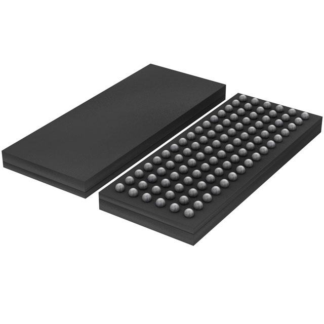
The onsemi 74LCX32245GX is a low voltage 32-bit bidirectional transceiver with 5V tolerant inputs and outputs. It contains thirty-two non-inverting buffers with 3-STATE outputs, designed for bus-oriented applications in 2.5V or 3.3V VCC environments interfacing to 5V signals. The device features byte control with separate inputs for four bytes, supporting live insertion/withdrawal. Packaged in a 96-ball Fine-Pitch Ball Grid Array (FBGA), it operates within a supply voltage range of 2.0V to 3.6V and an ambient temperature range of -40°C to +85°C.
Verify component authenticity as this part number may be obsolete. Confirm package integrity upon receipt, specifically checking for damage to the 96-ball FBGA structure. Ensure storage conditions adhere to moisture sensitivity level requirements before reflow soldering. Cross-reference ordering codes carefully, noting that suffixes indicate specific packaging variations such as trays or tape and reel formats.
Select this component when designing systems that require bidirectional data transfer between 2.5V or 3.3V logic and 5V tolerant buses. It is suitable for applications needing byte-wise control rather than full-word control. Consider the 96-ball FBGA package constraints regarding PCB layout and thermal management. Verify that the operating voltage range aligns with the system's power supply specifications.
This device belongs to the LCX family of low voltage CMOS logic components. It serves as a specialized transceiver for managing data flow across voltage boundaries. The 96-ball FBGA package provides a compact solution for high-density board designs. Its design focuses on minimizing power consumption while ensuring reliable signal transmission in mixed-voltage environments.
Public confirmed substitute part numbers include 74LCX16245MTDX, 74LVCH32245ABFG, and 74LVCH32245ABFG8.
The device supports live insertion and withdrawal provided the Output Enable (OE) input is tied to VCC through a pull-up resistor to ensure a high-impedance state during power up or down.
The maximum propagation delay (tPD) is 4.5 ns when the supply voltage (VCC) is 3.3V.
 74LCX32245GX
The activity of extra discounts on wholesale prices is in full swing…
Please fill in your contact information and we will send you the latest wholesale price list.