 ChipApex | Global Electronic Components Supplier

SEARCH
Search Product
Search Post
— IC芯片 | 连接器 | 传感器 | 被动器件 —
Search productSearch post
— IC芯片 | 连接器 | 传感器 | 被动器件 —
Consult the customer manager about the wholesale price.
consultation hotline:86-132-6715-2157
email:[email protected]
Contact the product manager for consultation. One-stop consultation is available.
Do you want a lower wholesale price? Please send us your inquiry and we will reply immediately.
74LV165D/AUJ is listed in the Shift Registers range at ChipApex. The manufacturer field lists NXP USA Inc.. Its product description is IC SHIFT REGISTER 8BIT 16SOIC. Review the specifications below when checking this part for your BOM.
The 74LV165D/AUJ is an 8-bit parallel-in/serial-out shift register manufactured by Nexperia. It features a serial data input (DS), eight parallel data inputs (D0 to D7), and two complementary serial outputs (Q7 and Q7). The device operates with a wide supply voltage range from 1.0 V to 5.5 V and includes clamp diodes on inputs for interfacing with voltages exceeding VCC. Data is loaded asynchronously when the parallel load input (PL) is LOW, while shifting occurs on LOW-to-HIGH clock transitions when the clock enable (CE) is LOW.
Verify that the specific ordering suffix matches the required package type, as the datasheet lists distinct packages such as SO16 (SOT109-1) and TSSOP16 (SOT403-1). Confirm the temperature range specification aligns with operational requirements, noting the standard -40 °C to +125 °C rating. Ensure compliance with JEDEC standards relevant to the target voltage domain before finalizing procurement.
Select this component for designs requiring low power CMOS dissipation and compatibility with mixed voltage environments. The device supports operation across multiple JEDEC standards, making it suitable for applications ranging from 1.65 V to 5.5 V. Consider the available ESD protection ratings and latch-up performance when evaluating robustness for industrial or automotive-grade environments.
This part belongs to the 74LV165 family of 8-bit shift registers produced by Nexperia. The manufacturer previously operated under NXP Semiconductors, which explains the brand association. The product is designed for general-purpose logic applications requiring reliable serial data handling with low power consumption and broad voltage tolerance.
The 74LV165PW is a verified alternative offering the same functionality in a TSSOP16 package instead of the SO16 variant. Both devices share identical electrical characteristics and pin configurations, allowing for potential form-factor adjustments without circuit redesign.
When the PL input is LOW, data from the parallel inputs (D0 to D7) is loaded into the shift register asynchronously. When PL is HIGH, data enters the register serially at the DS input.
The CE input controls the clocking action. When CE is LOW, data shifts on the LOW-to-HIGH transitions of the CP input. A HIGH level on CE disables the CP input, inhibiting serial shifting.
Explore related parts through Logic, Integrated Circuits (ICs), all product categories, ChipApex homepage.
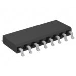 74LV165D/AUJ

74LV165D/AUJ is listed in the Shift Registers range at ChipApex. The manufacturer field lists NXP USA Inc.. Its product description is IC SHIFT REGISTER…
Read More
74LV165D/AUJ is listed in the Shift Registers range at ChipApex. The manufacturer field lists NXP USA Inc.. Its product description is IC SHIFT REGISTER…
Read More
Select a common mode choke using noise frequency, current, insulation and signal integrity. Understand impedance curves, layout and filter limitations.
Read More
Compare RC, crystal and MEMS oscillator circuits. Check ppm, jitter, load capacitance, startup margin and output compatibility before choosing a clock source.
Read More
74LV165D/AUJ is listed in the Shift Registers range at ChipApex. The manufacturer field lists NXP USA Inc.. Its product description is IC SHIFT REGISTER…
Read More
74LV165D/AUJ is listed in the Shift Registers range at ChipApex. The manufacturer field lists NXP USA Inc.. Its product description is IC SHIFT REGISTER…
Read More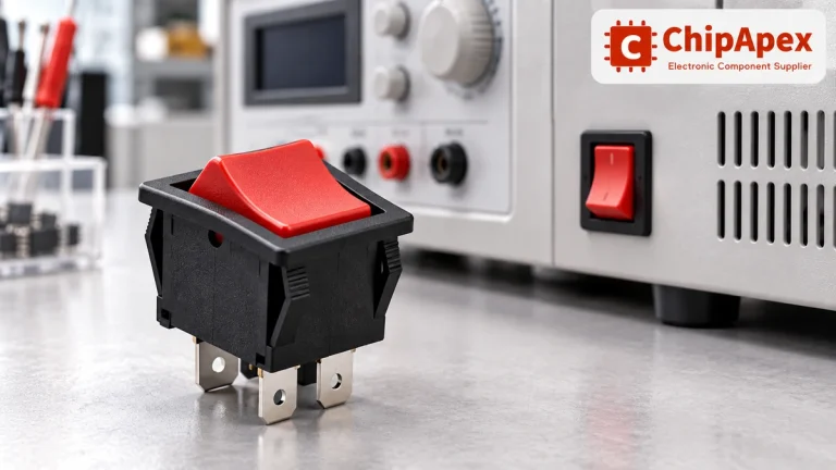
Choose a rocker switch by AC/DC ratings, contact arrangement, illumination, panel fit and sealing. Get practical checks for engineering and component sourcing.
Read More
74LV165D/AUJ is listed in the Shift Registers range at ChipApex. The manufacturer field lists NXP USA Inc.. Its product description is IC SHIFT REGISTER…
Read More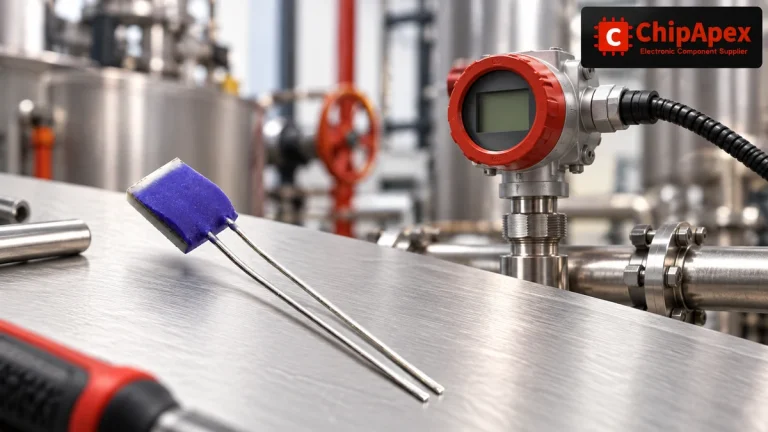
Compare Pt100 and Pt1000 RTDs, two-, three- and four-wire connections, excitation and self-heating. Build an error budget from element to reported temperature.
Read More74LV165D/AUJ is listed in the Shift Registers range at ChipApex. The manufacturer field lists NXP USA Inc.. Its product description is IC SHIFT REGISTER…
Read More
Choose LED drivers by current, string voltage, dimming and thermal limits. Understand constant-current operation and the checks needed for your load.
Read More
Understand how a comparator switches at a voltage threshold, why hysteresis prevents chatter, and which output and input specs matter.
Read More
The activity of extra discounts on wholesale prices is in full swing…
Please fill in your contact information and we will send you the latest wholesale price list.





