 ChipApex | Global Electronic Components Supplier

SEARCH
Search Product
Search Post
— IC芯片 | 连接器 | 传感器 | 被动器件 —
Search productSearch post
— IC芯片 | 连接器 | 传感器 | 被动器件 —
Consult the customer manager about the wholesale price.
consultation hotline:86-132-6715-2157
email:[email protected]
Contact the product manager for consultation. One-stop consultation is available.
Do you want a lower wholesale price? Please send us your inquiry and we will reply immediately.
74LV251PW,112 is listed in the Signal Switches, Multiplexers, Decoders range at ChipApex. The manufacturer field lists NXP USA Inc.. Its product description is IC MULTIPLEXER 1 X 8:1 16TSSOP. Review the specifications below when checking this part for your BOM.
The NXP USA Inc. 74LV251PW,112 is an 8-input multiplexer with 3-State outputs housed in a 16-pin TSSOP package. It operates within a supply voltage range of 1.0 V to 3.6 V and accepts TTL input levels between 2.7 V and 3.6 V. The device features true and complement outputs, both capable of high-impedance states for expansion. Typical propagation delays from inputs to outputs are 14 ns at 3.3 V with 15 pF load capacitance. Input capacitance is typically 3.5 pF, and power dissipation capacitance is 44 pF.
Verify the specific ordering suffix matches the required package type, as the 74LV251 family includes DIL, SO, SSOP, and TSSOP variants. Confirm temperature range requirements against the -40°C to +125°C specification. Ensure supply voltage constraints align with the 1.0 V to 3.6 V operating limits before procurement.
Select this component when an 8-to-1 multiplexer with tri-state outputs is required in a low-voltage environment. It is functionally compatible with 74HC/HCT251 devices but optimized for lower supply voltages down to 1.0 V. Consider the TSSOP package dimensions if space-constrained surface mount assembly is necessary.
This device belongs to the 74LV series of low-voltage CMOS logic integrated circuits manufactured by Philips Semiconductors (now NXP). The 74LV251 specifically implements an 8-input multiplexer architecture. It supersedes earlier data specifications from April 1997 and was published as a product specification in May 1998.
When the OE input is HIGH, both the Y and Y outputs enter a high impedance OFF-state. When OE is LOW, the selected input is routed to the outputs.
Yes, the inputs include clamp diodes which permit the use of current limiting resistors to interface inputs to voltages in excess of VCC.
Explore related parts through Logic, Integrated Circuits (ICs), all product categories, ChipApex homepage.
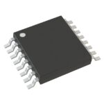 74LV251PW,112

74LV251PW,112 is listed in the Signal Switches, Multiplexers, Decoders range at ChipApex. The manufacturer field lists NXP USA Inc.. Its product description is IC…
Read More
74LV251PW,112 is listed in the Signal Switches, Multiplexers, Decoders range at ChipApex. The manufacturer field lists NXP USA Inc.. Its product description is IC…
Read More
See how a MEMS gyroscope measures angular rate, why its angle estimate drifts, and which range, noise, interface and temperature specs to compare.
Read More
74LV251PW,112 is listed in the Signal Switches, Multiplexers, Decoders range at ChipApex. The manufacturer field lists NXP USA Inc.. Its product description is IC…
Read More
74LV251PW,112 is listed in the Signal Switches, Multiplexers, Decoders range at ChipApex. The manufacturer field lists NXP USA Inc.. Its product description is IC…
Read More
74LV251PW,112 is listed in the Signal Switches, Multiplexers, Decoders range at ChipApex. The manufacturer field lists NXP USA Inc.. Its product description is IC…
Read More
74LV251PW,112 is listed in the Signal Switches, Multiplexers, Decoders range at ChipApex. The manufacturer field lists NXP USA Inc.. Its product description is IC…
Read More
74LV251PW,112 is listed in the Signal Switches, Multiplexers, Decoders range at ChipApex. The manufacturer field lists NXP USA Inc.. Its product description is IC…
Read More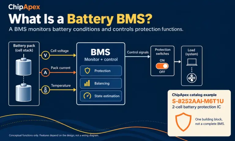
Learn what a battery BMS does, how protection differs from charging, and which pack specifications to check when sourcing BMS components through ChipApex.
Read More
74LV251PW,112 is listed in the Signal Switches, Multiplexers, Decoders range at ChipApex. The manufacturer field lists NXP USA Inc.. Its product description is IC…
Read More
74LV251PW,112 is listed in the Signal Switches, Multiplexers, Decoders range at ChipApex. The manufacturer field lists NXP USA Inc.. Its product description is IC…
Read More
74LV251PW,112 is listed in the Signal Switches, Multiplexers, Decoders range at ChipApex. The manufacturer field lists NXP USA Inc.. Its product description is IC…
Read More
The activity of extra discounts on wholesale prices is in full swing…
Please fill in your contact information and we will send you the latest wholesale price list.





