 ChipApex | Global Electronic Components Supplier
74LVC4T3144PW-Q10J
Search Product
Search Post
— IC芯片 | 连接器 | 传感器 | 被动器件 —
Search productSearch post
— IC芯片 | 连接器 | 传感器 | 被动器件 —
Consult the customer manager about the wholesale price.
consultation hotline:86-132-6715-2157
email:[email protected]
Contact the product manager for consultation. One-stop consultation is available.
Do you want a lower wholesale price? Please send us your inquiry and we will reply immediately.
The Nexperia 74LVC4T3144PW-Q10J is a 4-bit dual-supply level translating buffer with 3-state outputs, qualified to AEC-Q100 Grade 1. It features VCC(A) and VCC(B) supply voltage ranges of 1.2 V to 5.5 V. The device translates three inputs from VCC(A) to VCC(B) and one input from VCC(B) to VCC(A). It supports maximum data rates up to 200 Mbps at 3.3 V to 5.0 V translation. Operating temperatures range from -40 °C to +125 °C in the TSSOP14 package.
Verify the specific ordering suffix matches the required temperature range and package variant. Confirm that the Q100 designation aligns with automotive qualification requirements for your target application. Ensure compatibility with the TSSOP14 footprint and pinout configuration during PCB layout review.
Select this component when interfacing digital signals between two independent power domains requiring unidirectional translation. The asymmetric pin configuration allows three channels to translate from port A to B and one channel from B to A. Verify that the required data rate and supply voltage combinations fall within the specified dynamic characteristic limits.
This part belongs to the Nexperia 74LVC family of low-voltage CMOS logic devices. The 74LVC4T3144 series provides dual-supply buffering capabilities specifically designed for mixed-voltage system architectures. The Q100 suffix indicates automotive-grade manufacturing and testing protocols distinct from standard commercial variants.
Direct substitutes include the non-automotive 74LVC4T3144PW and other 74LVC4T3144 variants within the same family. Verify functional equivalence regarding the asymmetric input/output mapping and 3-state control logic before substitution.
The integrated IOFF circuitry disables the outputs to prevent damaging backflow current. If either VCC(A) or VCC(B) drops to GND, the device enters suspend mode and all outputs assume a high-impedance state.
Three inputs (A1, A2, A3) translate from VCC(A) to VCC(B), while one input (B4) translates from VCC(B) to VCC(A). The corresponding outputs follow these respective voltage references.
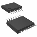 74LVC4T3144PW-Q10J
The activity of extra discounts on wholesale prices is in full swing…
Please fill in your contact information and we will send you the latest wholesale price list.





