 ChipApex | Global Electronic Components Supplier
8T49N240-027NLGI
Search Product
Search Post
— IC芯片 | 连接器 | 传感器 | 被动器件 —
Search productSearch post
— IC芯片 | 连接器 | 传感器 | 被动器件 —
Consult the customer manager about the wholesale price.
consultation hotline:86-132-6715-2157
email:[email protected]
Contact the product manager for consultation. One-stop consultation is available.
Do you want a lower wholesale price? Please send us your inquiry and we will reply immediately.
The Renesas 8T49N240-027NLGI is a FemtoClock NG Universal Frequency Translator and Jitter Attenuator. It features four LVPECL/LVDS/HCSL outputs capable of generating frequencies up to 867 MHz from inputs up to 875 MHz. The device operates on a single supply voltage ranging from 2.375 V to 3.465 V with a typical operating current of 40 mA. Packaged in a 6x6 mm VFQFPN-40 format, it supports I2C programming and includes phase-slope limiting for hitless switching. It is designed for applications requiring precise clock generation and jitter cleaning within the -40°C to +85°C temperature range.
Verify the specific suffix '027' against official Renesas documentation to confirm factory pre-programmed frequency configurations. Confirm availability status as distribution channels may report limited stock or end-of-life transitions. Ensure the ordering code matches the required output levels and boot source settings defined in the datasheet.
Select this component when designing systems requiring low-jitter clock translation for high-speed serial interfaces. Verify that the required output frequencies fall within the 8 kHz to 867 MHz range. Ensure the design accommodates the 2.375 V to 3.465 V supply voltage and utilizes the I2C interface for configuration management.
This part belongs to the 8T49N240 series of FemtoClock NG devices. The family provides universal frequency translation capabilities for telecommunications and datacom equipment. The specific model integrates a fractional-feedback PLL and multiple output dividers to meet strict jitter compliance standards for various networking protocols.
Consult the official Renesas cross-reference guide for verified substitutes. Note that timing product lines may undergo manufacturer transitions; verify if alternative sources are available through authorized distributors or successor entities.
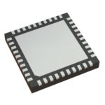 8T49N240-027NLGI
The activity of extra discounts on wholesale prices is in full swing…
Please fill in your contact information and we will send you the latest wholesale price list.






