 ChipApex | Global Electronic Components Supplier
9DB633AGLF
Search Product
Search Post
— IC芯片 | 连接器 | 传感器 | 被动器件 —
Search productSearch post
— IC芯片 | 连接器 | 传感器 | 被动器件 —
Consult the customer manager about the wholesale price.
consultation hotline:86-132-6715-2157
email:[email protected]
Contact the product manager for consultation. One-stop consultation is available.
Do you want a lower wholesale price? Please send us your inquiry and we will reply immediately.
The Renesas Electronics 9DB633AGLF is a PCI Express (PCIe) fanout buffer and zero-delay buffer integrated circuit. It features one differential input and six HCSL outputs, supporting maximum frequencies up to 110 MHz. The device operates within a supply voltage range of 3.135 V to 3.465 V and is housed in a 28-TSSOP package with a width of 4.40 mm. Designed for surface mount installation, it functions reliably across an operating temperature range of 0°C to +70°C. The component includes an internal Phase-Locked Loop (PLL) and complies with RoHS3 standards.
Verify the specific ordering suffix to confirm packaging format. The base part number 9DB633AGLF typically corresponds to tube packaging, whereas variants ending in 'T' indicate tape and reel options. Confirm the manufacturer's current production status and lead times directly with authorized distributors or Renesas Electronics prior to procurement planning.
Select this component when a single differential clock source must drive up to six downstream PCIe receivers with minimal skew. Ensure the design requires HCSL output logic levels and operates within the 0°C to +70°C commercial temperature range. Verify that the input frequency does not exceed the 110 MHz maximum specification for proper PLL operation.
This component belongs to the 9DB433/9DB633/9DB833 family of PCIe Gen3 buffers. While the 9DB433 provides four outputs and the 9DB833 offers eight, the 9DB633 specifically addresses designs requiring six buffered outputs. All members share similar electrical characteristics and are intended for high-speed serial interface timing applications.
Direct functional substitutes within the same family include the 9DB433AGLF (4 outputs) and 9DB833AGILF (8 outputs). Cross-family replacements require verification of pin compatibility and electrical specifications against the original design requirements.
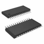 9DB633AGLF
The activity of extra discounts on wholesale prices is in full swing…
Please fill in your contact information and we will send you the latest wholesale price list.





