 ChipApex | Global Electronic Components Supplier
9DBL0243ANLGI8
Search Product
Search Post
— IC芯片 | 连接器 | 传感器 | 被动器件 —
Search productSearch post
— IC芯片 | 连接器 | 传感器 | 被动器件 —
Consult the customer manager about the wholesale price.
consultation hotline:86-132-6715-2157
email:[email protected]
Contact the product manager for consultation. One-stop consultation is available.
Do you want a lower wholesale price? Please send us your inquiry and we will reply immediately.
The 9DBL0243ANLGI8 is a 2-output low-power high-performance PCIe zero-delay/fanout clock buffer manufactured by Renesas Electronics Corporation. It supports PCIe Gen 1 through Gen 5 standards and operates at a supply voltage of 3.3V. The device features a typical power consumption of 100 mW and includes a Loss of Signal (LOS) detection function. It is housed in a VFQFPN package and utilizes tape and reel packaging for automated assembly.
Verify the specific ordering suffix NLGI8 confirms the VFQFPN package type and tape-and-reel delivery format. Ensure the component matches the 9DBL0243A family specifications, including the 3.3V operating voltage and LOS feature. Confirm that the source documentation explicitly identifies the manufacturer as Renesas Electronics Corporation to avoid counterfeits or incompatible variants.
Select this component when designing systems requiring zero-delay buffering for PCIe Gen 1 through Gen 5 applications. It is suitable for environments where low power consumption is critical, offering a typical draw of 100 mW. The integrated LOS detection provides additional system reliability. Ensure the design accommodates the VFQFPN package dimensions and thermal requirements specified in the official datasheet.
This part belongs to the 9DBL02x3/9DBL04x3/9DBL06x3/9DBL08x3 family of PCIe clock buffers from Renesas Electronics. These devices are engineered to provide high-performance clock distribution for PCI Express standards. The 9DBL0243 variant specifically offers two outputs, distinguishing it from higher-channel members of the same product line while maintaining consistent electrical characteristics and interface protocols.
Consult the official Renesas cross-reference documentation for verified substitutes within the 9DBL02x3 family. Direct replacements must maintain the 2-output configuration, 3.3V operation, and PCIe Gen 1–5 support. Verify package compatibility and pinout alignment before substitution.
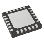 9DBL0243ANLGI8
The activity of extra discounts on wholesale prices is in full swing…
Please fill in your contact information and we will send you the latest wholesale price list.






