 ChipApex | Global Electronic Components Supplier
9DBL0653ANDGI8
Search Product
Search Post
— IC芯片 | 连接器 | 传感器 | 被动器件 —
Search productSearch post
— IC芯片 | 连接器 | 传感器 | 被动器件 —
Consult the customer manager about the wholesale price.
consultation hotline:86-132-6715-2157
email:[email protected]
Contact the product manager for consultation. One-stop consultation is available.
Do you want a lower wholesale price? Please send us your inquiry and we will reply immediately.
The 9DBL0653ANDGI8 is a zero-delay/fanout buffer IC designed for PCI Express (PCIe) applications, supporting Gen 1 through Gen 5 standards. It operates at a maximum frequency of 200MHz with one input and eight outputs. The device utilizes Low-Power HCSL (LP-HCSL) technology to eliminate external termination resistors. It is housed in a 40-VFQFPN (5x5mm) package and functions within a supply voltage range of 3.135V to 3.465V.
Verify the specific suffix 'ANDGI8' against official Renesas documentation to confirm package type and tape/reel specifications. Ensure compatibility with LP-HCSL signaling requirements for target designs. Confirm RoHS compliance status and moisture sensitivity level prior to integration into manufacturing processes.
Select this component for designs requiring high-speed PCIe clock fanout with minimal jitter. The integrated LP-HCSL outputs simplify PCB layout by removing the need for discrete termination resistors. Consider the 40-VFQFPN package constraints for thermal management and board space limitations.
This part belongs to the 9DBL0653 family of zero-delay buffers from Renesas Electronics. It is specifically engineered for PCIe clock generation and distribution, offering a compact solution for multi-lane interfaces. The device replaces older buffer solutions by integrating signal conditioning and distribution capabilities.
Public confirmed substitute: 9DBL0841BKILFT.
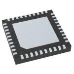 9DBL0653ANDGI8
The activity of extra discounts on wholesale prices is in full swing…
Please fill in your contact information and we will send you the latest wholesale price list.





