ChipApex | Global Electronic Components Supplier
9FGV1006B000LTGI
Search Product
Search Post
— IC芯片 | 连接器 | 传感器 | 被动器件 —
Search productSearch post
— IC芯片 | 连接器 | 传感器 | 被动器件 —
Consult the customer manager about the wholesale price.
consultation hotline:86-132-6715-2157
email:[email protected]
Contact the product manager for consultation. One-stop consultation is available.
Do you want a lower wholesale price? Please send us your inquiry and we will reply immediately.
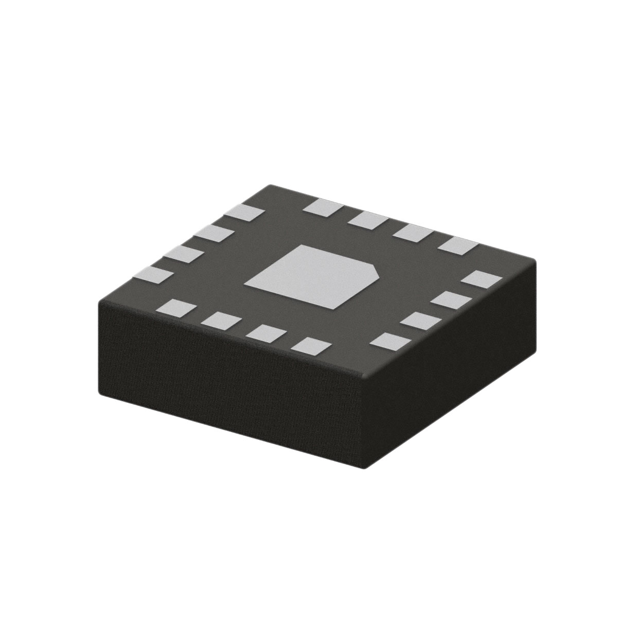
The 9FGV1006B000LTGI is a programmable clock generator from the Renesas PhiClock family, designed for high-performance timing applications. It features two output channels capable of generating frequencies up to 325 MHz with input frequencies reaching 240 MHz. The device supports LP-HCSL and LVDS output signaling types, operating within a supply voltage range of 1.71 V to 3.465 V. Packaged in a 16-LGA (3x3 mm) format, it functions across an industrial temperature range of -40°C to +85°C. This component integrates PLL technology to provide precise clock distribution for digital systems requiring low jitter and flexible configuration options.
Verify the specific suffix 'B000' against official Renesas documentation to confirm pinout and electrical characteristics, as variations exist within the 9FGV1006 series. Check moisture sensitivity level (MSL) ratings before storage and handling. Confirm availability status directly with authorized distributors, as lead times may vary based on production cycles. Ensure ESD protection measures are followed during assembly due to the small form factor.
Select this component when dual differential or single-ended outputs are required for PCIe or NVMe architectures. Compare output impedance requirements; LP-HCSL outputs typically offer 85-ohm termination. Evaluate jitter performance specifications against system tolerance limits. Consider I2C configurability if dynamic frequency changes are needed versus fixed hardware configurations. Verify power supply voltage compatibility with the 1.71V to 3.465V operating range.
This part belongs to the Renesas PhiClock™ programmable clock generator family, which includes variants like 9FGV1001 through 9FGV1006. These devices are optimized for PCI Express and NVMe applications, offering flexibility in clock generation compared to fixed-frequency oscillators. The 9FGV1006 series specifically targets high-speed serial interfaces requiring precise timing and low phase noise.
Direct substitutes within the same family include other 9FGV1006 variants with different output configurations or frequencies. Cross-reference pinouts and electrical parameters carefully when considering alternative manufacturers. Verify that any replacement maintains compatibility with the target system's voltage levels and signal integrity requirements.
 9FGV1006B000LTGI
The activity of extra discounts on wholesale prices is in full swing…
Please fill in your contact information and we will send you the latest wholesale price list.