 ChipApex | Global Electronic Components Supplier

SEARCH
Search Product
Search Post
— IC芯片 | 连接器 | 传感器 | 被动器件 —
Search productSearch post
— IC芯片 | 连接器 | 传感器 | 被动器件 —
Consult the customer manager about the wholesale price.
consultation hotline:86-132-6715-2157
email:[email protected]
Contact the product manager for consultation. One-stop consultation is available.
Do you want a lower wholesale price? Please send us your inquiry and we will reply immediately.
AD587JRZ-REEL is listed in the Voltage Reference range at ChipApex. The manufacturer field lists Analog Devices Inc.. Its product description is IC VREF SERIES 0.1% 8SOIC. Review the specifications below when checking this part for your BOM.
The AD587JRZ-REEL is a high precision monolithic voltage reference providing a nominal 10.000 V output. It utilizes an ion-implanted buried Zener diode and laser-trimmed thin-film resistors to achieve low noise and drift. The device operates within a temperature range of 0°C to 70°C with a maximum initial accuracy of 10 mV and a temperature coefficient of 20 ppm/°C. It features a dedicated noise reduction pin, optional fine trim capability, and requires a maximum quiescent current of 4 mA.
Verify the specific grade suffix (J, K, or U) to confirm the required temperature range and accuracy specifications. Ensure the package option matches the design requirements, as the JRZ variant indicates surface mount SOIC packaging. Confirm RoHS compliance status if environmental regulations apply to the manufacturing process. Cross-reference the ordering guide to ensure the reel quantity and tape specifications align with assembly equipment capabilities.
Select this component when system requirements demand superior noise performance and stability compared to standard on-chip references. The J grade offers a cost-effective solution for commercial temperature ranges, while the U grade supports extended industrial environments. Consider the available fine trim pin if the application requires output voltage adjustment beyond the factory laser trimming limits. Evaluate the need for the noise reduction pin based on the sensitivity of the connected analog-to-digital converter.
The AD587 series represents a significant advancement in monolithic voltage reference technology by employing a proprietary buried Zener diode. This design methodology yields significantly lower noise and thermal drift than conventional band gap references. The device maintains an industry-standard pinout, facilitating direct upgrades in existing systems that previously utilized older 10 V reference architectures.
AD587JRZ
The device includes a dedicated Noise Reduction pin that can be connected to ground via an external capacitor. This configuration forms a low-pass filter with internal resistances to attenuate high-frequency noise generated by the buried Zener diode.
The TRIM pin provides an optional fine-tuning capability for the output voltage. It allows users to offset the output by up to 300 mV to match a main system reference or accommodate binary application requirements such as 10.24 V.
Explore related parts through Power Management (PMIC), Integrated Circuits (ICs), all product categories, ChipApex homepage.
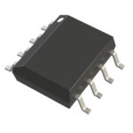 AD587JRZ-REEL
Explore electronic component types, functions, packages and datasheets. Learn selection, replacement and BOM checks before ordering parts for your PCB.
Read More
AD587JRZ-REEL is listed in the Voltage Reference range at ChipApex. The manufacturer field lists Analog Devices Inc.. Its product description is IC VREF SERIES…
Read More
AD587JRZ-REEL is listed in the Voltage Reference range at ChipApex. The manufacturer field lists Analog Devices Inc.. Its product description is IC VREF SERIES…
Read More
AD587JRZ-REEL is listed in the Voltage Reference range at ChipApex. The manufacturer field lists Analog Devices Inc.. Its product description is IC VREF SERIES…
Read More
AD587JRZ-REEL is listed in the Voltage Reference range at ChipApex. The manufacturer field lists Analog Devices Inc.. Its product description is IC VREF SERIES…
Read More
AD587JRZ-REEL is listed in the Voltage Reference range at ChipApex. The manufacturer field lists Analog Devices Inc.. Its product description is IC VREF SERIES…
Read More
AD587JRZ-REEL is listed in the Voltage Reference range at ChipApex. The manufacturer field lists Analog Devices Inc.. Its product description is IC VREF SERIES…
Read More
AD587JRZ-REEL is listed in the Voltage Reference range at ChipApex. The manufacturer field lists Analog Devices Inc.. Its product description is IC VREF SERIES…
Read More
Compare RC, crystal and MEMS oscillator circuits. Check ppm, jitter, load capacitance, startup margin and output compatibility before choosing a clock source.
Read More
Choose an AC to DC converter by input range, output demand, isolation, efficiency and thermal derating. Compare architectures and check installation needs.
Read More
Choose a DIP switch by contact type, coded positions, footprint and signal ratings. Check logic polarity, assembly conditions and PCB configuration behavior.
Read More
AD587JRZ-REEL is listed in the Voltage Reference range at ChipApex. The manufacturer field lists Analog Devices Inc.. Its product description is IC VREF SERIES…
Read More
The activity of extra discounts on wholesale prices is in full swing…
Please fill in your contact information and we will send you the latest wholesale price list.







