 ChipApex | Global Electronic Components Supplier
AD9525BCPZ
Search Product
Search Post
— IC芯片 | 连接器 | 传感器 | 被动器件 —
Search productSearch post
— IC芯片 | 连接器 | 传感器 | 被动器件 —
Consult the customer manager about the wholesale price.
consultation hotline:86-132-6715-2157
email:[email protected]
Contact the product manager for consultation. One-stop consultation is available.
Do you want a lower wholesale price? Please send us your inquiry and we will reply immediately.
The AD9525BCPZ is a low jitter clock generator featuring eight differential LVPECL outputs and an integrated ultralow noise synthesizer. It supports frequencies up to 3.6 GHz on the VCO input and all outputs, utilizing an external VCO or VCXO with an on-chip PLL. The device includes two differential reference inputs (REFA, REFB) and one single-ended input (REFC). It operates from a single 3.3 V supply for logic and allows VDD_CP up to 5.25 V. Configuration is managed via a SPI serial control port. The component is housed in a 48-lead LFCSP package and functions within an industrial temperature range of −40°C to +85°C.
Verify the specific suffix BCPZ corresponds to the standard 48-lead LFCSP package variant when sourcing. Confirm that the required external VCO or VCXO voltage does not exceed the 5.25 V limit for the VDD_CP pin. Ensure the design accommodates the necessary external resistors for OUT_RSET (4.12 kΩ) and CP_RSET (5.1 kΩ) as specified in the electrical characteristics table.
Select this component when sub-picosecond jitter performance is critical for multi-output distribution. The AD9525 requires an external VCO or VCXO; internal oscillators are not present. Designers must account for the separate VDD3 (3.3 V) and VDD_CP (up to 5.25 V) power domains. The common divider applies to all eight outputs, limiting independent frequency scaling per channel but ensuring matched skew across the output set.
The AD9525 belongs to Analog Devices' family of low jitter clock generators designed for demanding communication and test applications. Unlike devices with internal VCOs, it relies on external resonant circuits for frequency generation while providing robust distribution capabilities. The BCPZ designation identifies the lead-free, RoHS-compliant version in the LFCSP package, distinct from reel-based packaging variants like the -RL7 suffix.
Public confirmed substitute part numbers are not available in the provided documentation.
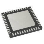 AD9525BCPZ
The activity of extra discounts on wholesale prices is in full swing…
Please fill in your contact information and we will send you the latest wholesale price list.






