 ChipApex | Global Electronic Components Supplier

SEARCH
Search Product
Search Post
— IC芯片 | 连接器 | 传感器 | 被动器件 —
Search productSearch post
— IC芯片 | 连接器 | 传感器 | 被动器件 —
Consult the customer manager about the wholesale price.
consultation hotline:86-132-6715-2157
email:[email protected]
Contact the product manager for consultation. One-stop consultation is available.
Do you want a lower wholesale price? Please send us your inquiry and we will reply immediately.
ADC1207S080HW/C1,5 is listed in the Analog To Digital Converters (ADC) range at ChipApex. The manufacturer field lists NXP USA Inc.. Its product description is IC ADC 12BIT 48HTQFP. Review the specifications below when checking this part for your BOM.
The ADC1207S080 is a single 12-bit Analog-to-Digital Converter (ADC) optimized for direct Input Frequency (IF) sampling in ultra-high IF radio transceivers. It operates at a maximum sampling rate of 80 MHz with a differential input bandwidth of 375 MHz. The device features an internal front-end buffer providing less than 1 pF input capacitance, enabling flexible aliasing filter strategies. It supports full-scale adjustment from 1.5 V to 2 V peak-to-peak and utilizes a single 5 V analog/digital supply alongside a 3.3 V LVCMOS output supply. Key performance metrics include 90 dB SFDR at 225 MHz input frequency and 74 dB SFDR at 175 MHz.
Verify the package type HTQFP48 (SOT545-2) matches design requirements. Confirm supply voltage conditions: VCCA/VCCD at 5.0 V nominal and VCCO at 3.3 V nominal. Ensure thermal management accounts for total power dissipation up to 990 mW at maximum clock rates. Check for industrial temperature range compliance (-40 °C to +85 °C).
Select this component for applications requiring direct high-frequency IF sampling without intermediate mixing stages. The low input capacitance (< 1 pF) simplifies front-end filter design. Ensure the system can provide stable 5 V analog/digital supplies and 3.3 V logic levels. Consider the 2-cycle latency and programmable CCS delay for precise data acquisition timing alignment.
The ADC1207S080 belongs to NXP's portfolio of high-performance data converters designed for telecommunications. It is housed in a 48-lead HTQFP48 plastic thermal enhanced thin quad flat package with an exposed die pad for improved thermal dissipation. The device is part of a series optimized for cellular infrastructure and wireless LAN applications.
Publicly confirmed substitute part numbers are not available in the provided documentation. Designers should consult NXP Semiconductors directly for current alternative product recommendations or cross-reference options.
The full-scale input voltage is continuously adjustable from 1.5 V to 2 V peak-to-peak by connecting an external reference voltage to the FSIN pin.
The ADC supports PECL mode 1, PECL mode 2, PECL mode 3, Differential AC driving mode, and TTL mode, allowing flexibility in clock source integration.
The Complete Conversion Signal (CCS) is a programmable output that indicates when conversion is complete. Its delay can be adjusted using DEL0 and DEL1 inputs to optimize data acquisition timing.
Explore related parts through Data Acquisition, Integrated Circuits (ICs), all product categories, ChipApex homepage.
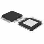 ADC1207S080HW/C1,5

ADC1207S080HW/C1,5 is listed in the Analog To Digital Converters (ADC) range at ChipApex. The manufacturer field lists NXP USA Inc.. Its product description is…
Read More
Understand how oscillators generate timing signals, how they differ from crystals, and which frequency, output and stability specs matter when choosing one.
Read More
ADC1207S080HW/C1,5 is listed in the Analog To Digital Converters (ADC) range at ChipApex. The manufacturer field lists NXP USA Inc.. Its product description is…
Read More
Compare Pt100 and Pt1000 RTDs, two-, three- and four-wire connections, excitation and self-heating. Build an error budget from element to reported temperature.
Read More
ADC1207S080HW/C1,5 is listed in the Analog To Digital Converters (ADC) range at ChipApex. The manufacturer field lists NXP USA Inc.. Its product description is…
Read More
ADC1207S080HW/C1,5 is listed in the Analog To Digital Converters (ADC) range at ChipApex. The manufacturer field lists NXP USA Inc.. Its product description is…
Read More
ADC1207S080HW/C1,5 is listed in the Analog To Digital Converters (ADC) range at ChipApex. The manufacturer field lists NXP USA Inc.. Its product description is…
Read More
Learn the relay definition, coil and contact operation, NO and NC forms, load ratings and suppression choices. Compare mechanical, reed and solid-state types.
Read More
ADC1207S080HW/C1,5 is listed in the Analog To Digital Converters (ADC) range at ChipApex. The manufacturer field lists NXP USA Inc.. Its product description is…
Read More
ADC1207S080HW/C1,5 is listed in the Analog To Digital Converters (ADC) range at ChipApex. The manufacturer field lists NXP USA Inc.. Its product description is…
Read More
ADC1207S080HW/C1,5 is listed in the Analog To Digital Converters (ADC) range at ChipApex. The manufacturer field lists NXP USA Inc.. Its product description is…
Read More
ADC1207S080HW/C1,5 is listed in the Analog To Digital Converters (ADC) range at ChipApex. The manufacturer field lists NXP USA Inc.. Its product description is…
Read More
The activity of extra discounts on wholesale prices is in full swing…
Please fill in your contact information and we will send you the latest wholesale price list.




