 ChipApex | Global Electronic Components Supplier

SEARCH
Search Product
Search Post
— IC芯片 | 连接器 | 传感器 | 被动器件 —
Search productSearch post
— IC芯片 | 连接器 | 传感器 | 被动器件 —
Consult the customer manager about the wholesale price.
consultation hotline:86-132-6715-2157
email:[email protected]
Contact the product manager for consultation. One-stop consultation is available.
Do you want a lower wholesale price? Please send us your inquiry and we will reply immediately.
ADC12SJ800AAVQ1 is listed in the Analog To Digital Converters (ADC) range at ChipApex. The manufacturer field lists Texas Instruments. Its product description is AUTOMOTIVE SINGLE-CHANNEL, 12-BI. Review the specifications below when checking this part for your BOM.
The ADC12SJ800AAVQ1 is a single-channel, 12-bit analog-to-digital converter (ADC) from Texas Instruments. It operates at a maximum sampling rate of 800MSPS and features a full-power input bandwidth of 6GHz. The device utilizes a non-interleaved architecture with an internal dither to reduce high-order harmonics. Performance specifications include a signal-to-noise ratio (SNR) of 57.6dBFS and an effective number of bits (ENOB) of 9 Bits at 97MHz. It supports JESD204C serial data interfaces with baud-rates up to 17.16Gbps and optional internal clock generation via a PLL and VCO operating between 7.2GHz and 8.2GHz. Power consumption at 800MSPS is 830mW, supplied by 1.1V and 1.9V rails.
Verify the specific ordering suffix against the manufacturer's official documentation to confirm package type and qualification grade. Ensure that any required export control documents are prepared prior to purchase, as this product may require additional files for export from the United States. Confirm compatibility with existing system power supplies and clocking infrastructure before finalizing procurement.
Select the ADC12SJ800AAVQ1 when a single-channel configuration is sufficient for the application, as it offers lower power consumption compared to dual or quad-channel variants. Consider the internal PLL capabilities if external high-frequency clocking hardware needs to be minimized. Verify that the 12-bit resolution and 800MSPS sampling rate align with the dynamic range and bandwidth requirements of the target signal processing chain.
This component belongs to the ADC12xJ800-Q1 family, which includes quad and dual-channel versions sharing similar core architectures. All variants in this series utilize the FCBGA-144 package and support the same JESD204C interface standards. The single-channel designation indicates dedicated analog inputs without shared resources found in multi-channel devices, optimizing performance for isolated signal paths.
The ADS5474-SP is documented as a pin-compatible alternative within the broader TI portfolio, though it differs significantly in resolution and technology. Direct functional replacements within the same family include the ADC12DJ800-Q1 and ADC12QJ800-Q1, provided channel count differences are acceptable. Verify electrical characteristics carefully when substituting across different channel counts.
The device supports a maximum SerDes baud-rate of 17.16Gbps.
An internal dither mechanism is included in the ADC core to reduce high-order harmonics.
Yes, it features an optional internal sampling clock generation block consisting of a PLL and a VCO operating between 7.2GHz and 8.2GHz.
Explore related parts through Data Acquisition, Integrated Circuits (ICs), all product categories, ChipApex homepage.
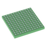 ADC12SJ800AAVQ1

Select a bridge rectifier by reverse voltage, capacitor charging current, startup surge and cooling. Work through a stated DC voltage and ripple example.
Read More
ADC12SJ800AAVQ1 is listed in the Analog To Digital Converters (ADC) range at ChipApex. The manufacturer field lists Texas Instruments. Its product description is AUTOMOTIVE…
Read More
Compare thermistors, RTDs, thermocouples and temperature ICs. Learn how range, accuracy, response, interfaces and mounting affect component selection.
Read More
ADC12SJ800AAVQ1 is listed in the Analog To Digital Converters (ADC) range at ChipApex. The manufacturer field lists Texas Instruments. Its product description is AUTOMOTIVE…
Read More
ADC12SJ800AAVQ1 is listed in the Analog To Digital Converters (ADC) range at ChipApex. The manufacturer field lists Texas Instruments. Its product description is AUTOMOTIVE…
Read More
ADC12SJ800AAVQ1 is listed in the Analog To Digital Converters (ADC) range at ChipApex. The manufacturer field lists Texas Instruments. Its product description is AUTOMOTIVE…
Read More
ADC12SJ800AAVQ1 is listed in the Analog To Digital Converters (ADC) range at ChipApex. The manufacturer field lists Texas Instruments. Its product description is AUTOMOTIVE…
Read More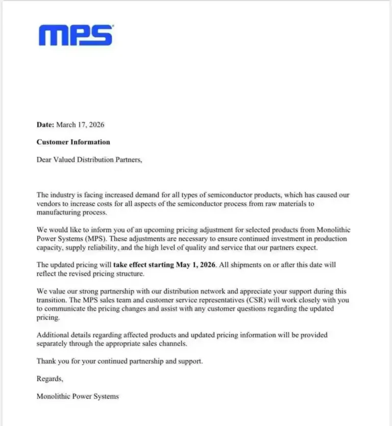
ADC12SJ800AAVQ1 is listed in the Analog To Digital Converters (ADC) range at ChipApex. The manufacturer field lists Texas Instruments. Its product description is AUTOMOTIVE…
Read More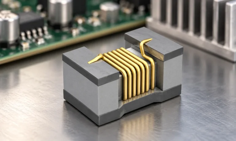
See when an inductor behaves linearly, how DC bias and saturation reduce inductance, and which current and temperature curves to check.
Read More
ADC12SJ800AAVQ1 is listed in the Analog To Digital Converters (ADC) range at ChipApex. The manufacturer field lists Texas Instruments. Its product description is AUTOMOTIVE…
Read More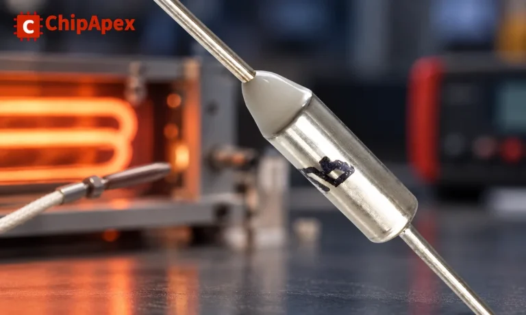
Understand thermal fuse operation, Tf, Th and Tm, electrical ratings and mounting. Check temperature limits and replacement requirements for your design.
Read More
ADC12SJ800AAVQ1 is listed in the Analog To Digital Converters (ADC) range at ChipApex. The manufacturer field lists Texas Instruments. Its product description is AUTOMOTIVE…
Read More
The activity of extra discounts on wholesale prices is in full swing…
Please fill in your contact information and we will send you the latest wholesale price list.





