 ChipApex | Global Electronic Components Supplier

SEARCH
Search Product
Search Post
— IC芯片 | 连接器 | 传感器 | 被动器件 —
Search productSearch post
— IC芯片 | 连接器 | 传感器 | 被动器件 —
Consult the customer manager about the wholesale price.
consultation hotline:86-132-6715-2157
email:[email protected]
Contact the product manager for consultation. One-stop consultation is available.
Do you want a lower wholesale price? Please send us your inquiry and we will reply immediately.
ASNT7121-KMA is listed in the Analog To Digital Converters (ADC) range at ChipApex. The manufacturer field lists ADSANTEC. Its product description is 20GH 15GS 4-BIT FLASH ADC W/ PLL. Review the specifications below when checking this part for your BOM.
The ASNT7121-KMA is a 4-bit flash analog-to-digital converter (ADC) with a sampling rate of 15 GS/s and an analog input bandwidth of 20 GHz. It features a selectable clocking mode using either an external high-speed clock or an internal PLL with a central frequency of 10 GHz. The device includes an on-chip 4-to-16 demultiplexer to reduce the output data rate to DC–3.75 Gbps. Power consumption is 2.8 W from a single +3.5 V supply, housed in a custom 100-pin metal-ceramic CQFP package.
Verify the specific revision level against the datasheet Rev. 1.5.2 February 2020. Confirm that the application board supports the custom 100-pin CQFP package and provides adequate thermal management for the center heat slug, as the junction-to-case thermal resistance is 4°C/W.
Select this component when a 4-bit resolution at 15 GS/s is required. Ensure the system can accommodate the 2.8 W power dissipation and provide a stable +3.5 V supply. Verify compatibility with the differential CML input requirements and the LVDS output interface standards.
Manufactured by Advanced Science And Novel Technology Company, Inc. (ADSANTEC), located in Torrance, California. The part number suffix KMA indicates the specific 100-pin metal-ceramic package configuration.
No public confirmed substitute part numbers are available in the provided documentation. Due to the proprietary nature of the flash ADC architecture and custom packaging, direct pin-compatible replacements are not documented.
These pins allow adjustment of the ADC threshold voltages. vrefcrl shifts the DC levels of all thresholds simultaneously, while vlsbcrl alters the voltage range of the least significant bit (LSB).
The CMU operates in two modes: clock multiplication (PLL on) which multiplies an external reference clock, or clock division (PLL off) which divides an external high-speed clock. Both modes generate internal clocks divided by 2, 4, 8, and 16.
The PRBS generator creates a 127-bit pseudo-random binary sequence to substitute encoded data, allowing for the alignment and testing of the output interface without requiring actual analog input signals.
Explore related parts through Data Acquisition, Integrated Circuits (ICs), all product categories, ChipApex homepage.
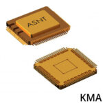 ASNT7121-KMA

ASNT7121-KMA is listed in the Analog To Digital Converters (ADC) range at ChipApex. The manufacturer field lists ADSANTEC. Its product description is 20GH 15GS…
Read More
Compare Pt100 and Pt1000 RTDs, two-, three- and four-wire connections, excitation and self-heating. Build an error budget from element to reported temperature.
Read More
Learn how rectifiers convert AC to DC, compare half-wave and bridge circuits, and select voltage, current, recovery and thermal ratings for your design.
Read More
ASNT7121-KMA is listed in the Analog To Digital Converters (ADC) range at ChipApex. The manufacturer field lists ADSANTEC. Its product description is 20GH 15GS…
Read More
ASNT7121-KMA is listed in the Analog To Digital Converters (ADC) range at ChipApex. The manufacturer field lists ADSANTEC. Its product description is 20GH 15GS…
Read More
ASNT7121-KMA is listed in the Analog To Digital Converters (ADC) range at ChipApex. The manufacturer field lists ADSANTEC. Its product description is 20GH 15GS…
Read More
ASNT7121-KMA is listed in the Analog To Digital Converters (ADC) range at ChipApex. The manufacturer field lists ADSANTEC. Its product description is 20GH 15GS…
Read More
ASNT7121-KMA is listed in the Analog To Digital Converters (ADC) range at ChipApex. The manufacturer field lists ADSANTEC. Its product description is 20GH 15GS…
Read More
ASNT7121-KMA is listed in the Analog To Digital Converters (ADC) range at ChipApex. The manufacturer field lists ADSANTEC. Its product description is 20GH 15GS…
Read More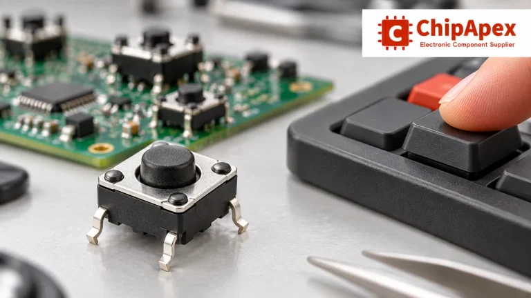
Choose tactile switches by operating force, travel, actuator height, footprint and lifetime. Check debounce, sealing and the assembled button mechanism.
Read More
ASNT7121-KMA is listed in the Analog To Digital Converters (ADC) range at ChipApex. The manufacturer field lists ADSANTEC. Its product description is 20GH 15GS…
Read More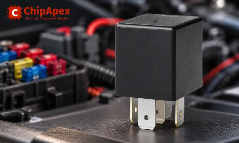
Learn the relay definition, coil and contact operation, NO and NC forms, load ratings and suppression choices. Compare mechanical, reed and solid-state types.
Read More
The activity of extra discounts on wholesale prices is in full swing…
Please fill in your contact information and we will send you the latest wholesale price list.




