 ChipApex | Global Electronic Components Supplier

SEARCH
Search Product
Search Post
— IC芯片 | 连接器 | 传感器 | 被动器件 —
Search productSearch post
— IC芯片 | 连接器 | 传感器 | 被动器件 —
Consult the customer manager about the wholesale price.
consultation hotline:86-132-6715-2157
email:[email protected]
Contact the product manager for consultation. One-stop consultation is available.
Do you want a lower wholesale price? Please send us your inquiry and we will reply immediately.
CBT3251D,118 is listed in the Signal Switches, Multiplexers, Decoders range at ChipApex. The manufacturer field lists Nexperia USA Inc.. Its product description is IC MUX/DEMUX 1 X 8:1 16SO. Review the specifications below when checking this part for your BOM.
The CBT3251D,118 is a single-pole, 8-throw bus switch manufactured by Nexperia USA Inc. It features an output enable input (OE) and three select inputs (S0, S1, S2). The device operates within a supply voltage range of 4.5 V to 5.5 V and supports an operating temperature range from -40 °C to +85 °C. Key electrical parameters include a maximum ON resistance of 7 Ω at VCC = 4.5 V and 15 Ω at VCC = 2.4 V. Propagation delay through the switch is specified as a maximum of 0.25 ns.
Verify the specific package variant during procurement, as the CBT3251 family includes both SO16 and TSSOP16 options. Confirm that the selected component matches the required temperature range and pin configuration for your design. Ensure all unused control inputs are properly terminated to VCC or GND to guarantee correct device functionality and avoid undefined states.
Select this component when a low-profile, high-speed 1-of-8 multiplexer is required for 5 V logic systems. Consider the SO16 package for standard surface-mount assembly needs. Evaluate the propagation delay and ON resistance specifications against your signal integrity requirements. Ensure the application environment stays within the specified -40 °C to +85 °C operating temperature limits.
This part belongs to the CBT series of bus switches designed for high-speed signal routing. It serves as a digital multiplexer/demultiplexer solution for connecting one common port to eight selectable ports. The device is intended for use in general-purpose digital applications requiring flexible signal path management within standard logic voltage domains.
Check for compatible parts within the same CBT family that offer identical pinouts and electrical characteristics. Verify that any substitute component maintains the same package type and thermal performance. Ensure the alternative device meets the required ESD protection levels and latch-up ratings specified for the original design.
When the Output Enable (OE) input is LOW, the switch is enabled, allowing the select inputs to route the A terminal to one of the B terminals. When OE is HIGH, the switch is disabled regardless of the select input states.
Pin 6 is designated as 'n.c.' (not connected). It has no internal electrical connection and should be left unconnected in the circuit layout.
The ON resistance is measured by the voltage drop between the A and Bn terminals at a specified current. The lowest voltage of the two terminals determines the ON resistance value.
Explore related parts through Logic, Integrated Circuits (ICs), all product categories, ChipApex homepage.
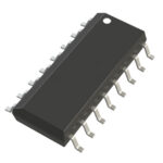 CBT3251D,118
Compare thermistors, RTDs, thermocouples and temperature ICs. Learn how range, accuracy, response, interfaces and mounting affect component selection.
Read More
CBT3251D,118 is listed in the Signal Switches, Multiplexers, Decoders range at ChipApex. The manufacturer field lists Nexperia USA Inc.. Its product description is IC…
Read More
CBT3251D,118 is listed in the Signal Switches, Multiplexers, Decoders range at ChipApex. The manufacturer field lists Nexperia USA Inc.. Its product description is IC…
Read More
CBT3251D,118 is listed in the Signal Switches, Multiplexers, Decoders range at ChipApex. The manufacturer field lists Nexperia USA Inc.. Its product description is IC…
Read More
Learn the relay definition, coil and contact operation, NO and NC forms, load ratings and suppression choices. Compare mechanical, reed and solid-state types.
Read More
CBT3251D,118 is listed in the Signal Switches, Multiplexers, Decoders range at ChipApex. The manufacturer field lists Nexperia USA Inc.. Its product description is IC…
Read More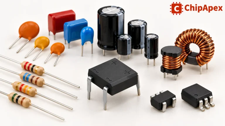
Explore electronic component types, functions, packages and datasheets. Learn selection, replacement and BOM checks before ordering parts for your PCB.
Read More
CBT3251D,118 is listed in the Signal Switches, Multiplexers, Decoders range at ChipApex. The manufacturer field lists Nexperia USA Inc.. Its product description is IC…
Read More
CBT3251D,118 is listed in the Signal Switches, Multiplexers, Decoders range at ChipApex. The manufacturer field lists Nexperia USA Inc.. Its product description is IC…
Read More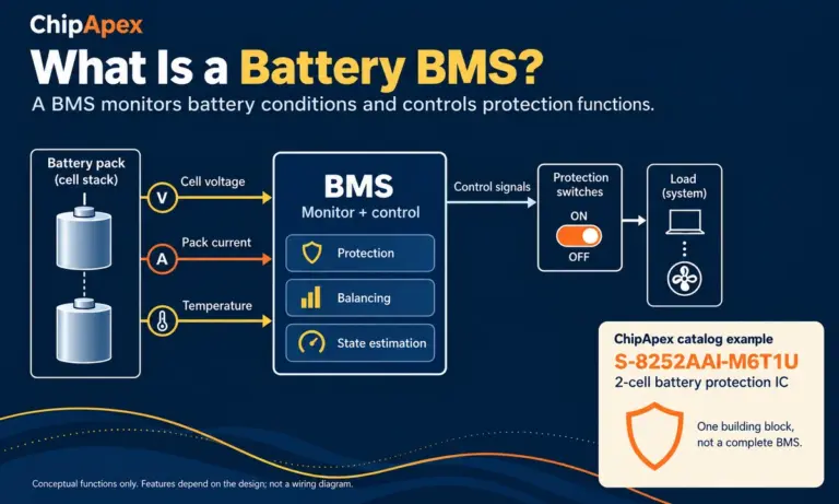
Learn what a battery BMS does, how protection differs from charging, and which pack specifications to check when sourcing BMS components through ChipApex.
Read More
CBT3251D,118 is listed in the Signal Switches, Multiplexers, Decoders range at ChipApex. The manufacturer field lists Nexperia USA Inc.. Its product description is IC…
Read More
CBT3251D,118 is listed in the Signal Switches, Multiplexers, Decoders range at ChipApex. The manufacturer field lists Nexperia USA Inc.. Its product description is IC…
Read More
The activity of extra discounts on wholesale prices is in full swing…
Please fill in your contact information and we will send you the latest wholesale price list.





