 ChipApex | Global Electronic Components Supplier

SEARCH
Search Product
Search Post
— IC芯片 | 连接器 | 传感器 | 被动器件 —
Search productSearch post
— IC芯片 | 连接器 | 传感器 | 被动器件 —
Consult the customer manager about the wholesale price.
consultation hotline:86-132-6715-2157
email:[email protected]
Contact the product manager for consultation. One-stop consultation is available.
Do you want a lower wholesale price? Please send us your inquiry and we will reply immediately.
CY2308ESXC-2 is listed in the Clock Generators, PLLs, Frequency Synthesizers range at ChipApex. The manufacturer field lists Infineon Technologies. Its product description is IC FANOUT BUFFER 16SOIC. Review the specifications below when checking this part for your BOM.
The CY2308ESXC-2 is a 3.3V Zero Delay Buffer manufactured by Infineon Technologies, originally designed by Cypress Semiconductor. It features an on-chip PLL that locks to an input clock presented on the REF pin, with feedback driven into the FBK pin from one of the outputs. The device provides eight low skew outputs organized into two banks of four, controlled by select inputs S1 and S2. It supports operating frequencies from 10 MHz to 133 MHz. The part is available in a 16-pin 150 mil SOIC package (SXC suffix) for commercial temperature range (0°C to 70°C).
Verify component authenticity through authorized distributors or official manufacturer channels. Confirm the specific ordering suffix matches the required package type and temperature rating. Check current availability status as this component may be subject to end-of-life restrictions or limited supply conditions.
Select the CY2308ESXC-2 when zero delay buffering with 2X frequency multiplication is required. Ensure the system load capacitance aligns with the specified limits for the target operating frequency. Verify that the 16-pin SOIC package fits the PCB layout constraints and that the commercial temperature range meets the application requirements.
This component belongs to the CY2308 family of 3.3V Zero Delay Buffers. The 'ESXC' designation indicates a 16-pin SOIC package with commercial temperature rating. Other variants in the series include different output configurations such as reference-only or 4X multiplication, and packages like TSSOP.
Direct substitutes within the same family include CY2308SC-2 for standard drive or CY2308SI-2 for industrial temperature. Cross-manufacturer equivalents like NB2308AI4D offer similar zero-delay buffer functionality but require verification of electrical characteristics and pin compatibility.
Zero input-output delay is achieved by closing the feedback loop where the FBK pin is driven from one of the outputs. The relative loading of this output compared to the remaining outputs adjusts the input-output delay.
The S1 and S2 inputs control the state of the output banks. They can enable or disable Bank A and Bank B, route the reference clock directly to outputs for testing, or shut down the PLL to reduce power consumption.
In the CY2308-2 configuration, connecting the feedback to Bank A provides Reference/2 on Bank B while Bank A runs at Reference. Connecting feedback to Bank B provides 2X Reference on Bank A while Bank B runs at Reference.
Explore related parts through Clock/Timing, Integrated Circuits (ICs), all product categories, ChipApex homepage.
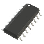 CY2308ESXC-2

See how a MEMS gyroscope measures angular rate, why its angle estimate drifts, and which range, noise, interface and temperature specs to compare.
Read More
CY2308ESXC-2 is listed in the Clock Generators, PLLs, Frequency Synthesizers range at ChipApex. The manufacturer field lists Infineon Technologies. Its product description is IC…
Read More
Compare thermistors, RTDs, thermocouples and temperature ICs. Learn how range, accuracy, response, interfaces and mounting affect component selection.
Read More
CY2308ESXC-2 is listed in the Clock Generators, PLLs, Frequency Synthesizers range at ChipApex. The manufacturer field lists Infineon Technologies. Its product description is IC…
Read More
Learn what an integrated circuit is, how ICs work, the main types and the specs to check before choosing a part for your design…
Read More
CY2308ESXC-2 is listed in the Clock Generators, PLLs, Frequency Synthesizers range at ChipApex. The manufacturer field lists Infineon Technologies. Its product description is IC…
Read More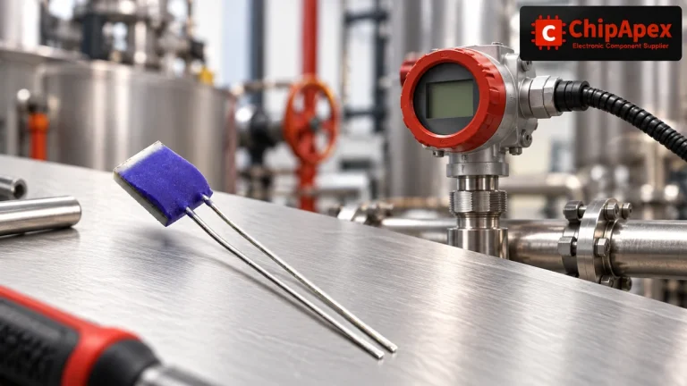
Compare Pt100 and Pt1000 RTDs, two-, three- and four-wire connections, excitation and self-heating. Build an error budget from element to reported temperature.
Read More
CY2308ESXC-2 is listed in the Clock Generators, PLLs, Frequency Synthesizers range at ChipApex. The manufacturer field lists Infineon Technologies. Its product description is IC…
Read More
CY2308ESXC-2 is listed in the Clock Generators, PLLs, Frequency Synthesizers range at ChipApex. The manufacturer field lists Infineon Technologies. Its product description is IC…
Read More
CY2308ESXC-2 is listed in the Clock Generators, PLLs, Frequency Synthesizers range at ChipApex. The manufacturer field lists Infineon Technologies. Its product description is IC…
Read More
Find out when a bare shock switch needs a pull resistor, when an MCU internal pull-up is enough, and why sensor modules and piezo…
Read More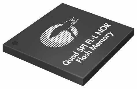
CY2308ESXC-2 is listed in the Clock Generators, PLLs, Frequency Synthesizers range at ChipApex. The manufacturer field lists Infineon Technologies. Its product description is IC…
Read More
The activity of extra discounts on wholesale prices is in full swing…
Please fill in your contact information and we will send you the latest wholesale price list.






