 ChipApex | Global Electronic Components Supplier

SEARCH
Search Product
Search Post
— IC芯片 | 连接器 | 传感器 | 被动器件 —
Search productSearch post
— IC芯片 | 连接器 | 传感器 | 被动器件 —
Consult the customer manager about the wholesale price.
consultation hotline:86-132-6715-2157
email:[email protected]
Contact the product manager for consultation. One-stop consultation is available.
Do you want a lower wholesale price? Please send us your inquiry and we will reply immediately.
CY7B9910-7SXCT is listed in the Clock Generators, PLLs, Frequency Synthesizers range at ChipApex. The manufacturer field lists Infineon Technologies. Its product description is IC FANOUT BUFFER 24SOIC. Review the specifications below when checking this part for your BOM.
The CY7B9910-7SXCT is a low skew clock buffer manufactured by Infineon Technologies (formerly Cypress Semiconductor). It features an integrated PLL for zero-delay operation and provides eight differential outputs. The device operates within a frequency range of 15 to 80 MHz, depending on the FS pin configuration. Key electrical parameters include a typical output skew of 0.3 ns and a maximum of 0.75 ns. Jitter specifications are limited to 200 ps peak-to-peak and 25 ps RMS. The component utilizes a 24-pin SOIC package and supports commercial temperature ranges.
Verify the specific suffix 'SXCT' corresponds to the tape and reel packaging variant listed in the official ordering information. Confirm that the manufacturer designation aligns with Infineon Technologies following their acquisition of Cypress Semiconductor assets. Ensure the component meets the required commercial operating temperature range before integration into the design.
Select this model when a low skew clock buffer with integrated PLL is required for frequencies up to 80 MHz. The -7 accuracy grade offers a typical skew of 0.3 ns, suitable for applications tolerating slightly higher skew than the -2 or -5 grades. Consider the 24-pin SOIC package constraints and ensure the PCB layout accommodates the necessary termination resistors for the 50Ω transmission lines.
This component belongs to the CY7B9910/CY7B9920 family of low skew clock buffers. The CY7B9910 variant specifically delivers TTL logic levels, whereas the CY7B9920 provides CMOS levels. Both share identical functional block diagrams and PLL capabilities, differing primarily in output drive characteristics and voltage thresholds.
Direct substitutes within the same family include CY7B9910-2SXCT and CY7B9910-5SXCT, which offer tighter skew specifications of 0.1 ns and 0.25 ns respectively. These alternatives maintain the same package and pinout but may require adjustments to timing budgets due to improved performance metrics.
The TEST input is a three-level input used for testing purposes. In normal operation, it is connected to ground. Forcing it to MID or HIGH disconnects the internal PLL, allowing the REF input to directly control all outputs while maintaining relative output-to-output functions.
The operating frequency range is selected via the FS (Frequency Select) pin. Setting FS to LOW allows 15-30 MHz, MID allows 25-50 MHz, and HIGH allows 40-80 MHz operation.
Yes, they can be connected in series to construct a board-to-board clock distribution tree. However, the datasheet advises against connecting more than two clock buffers in series due to jitter accumulation caused by non-ideal PLL filter characteristics.
Explore related parts through Clock/Timing, Integrated Circuits (ICs), all product categories, ChipApex homepage.
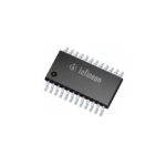 CY7B9910-7SXCT
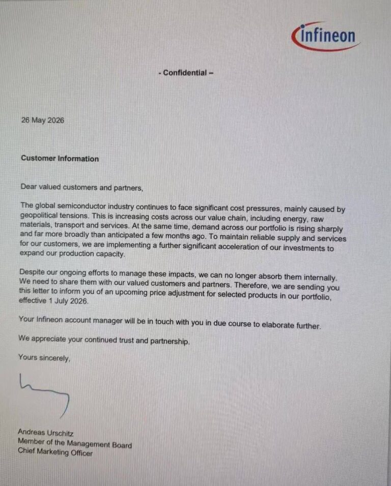
CY7B9910-7SXCT is listed in the Clock Generators, PLLs, Frequency Synthesizers range at ChipApex. The manufacturer field lists Infineon Technologies. Its product description is IC…
Read More
CY7B9910-7SXCT is listed in the Clock Generators, PLLs, Frequency Synthesizers range at ChipApex. The manufacturer field lists Infineon Technologies. Its product description is IC…
Read More
CY7B9910-7SXCT is listed in the Clock Generators, PLLs, Frequency Synthesizers range at ChipApex. The manufacturer field lists Infineon Technologies. Its product description is IC…
Read More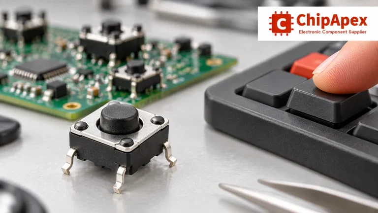
Understand tactile switches, PCB and keyboard differences, four-pin wiring, debounce, force, travel and replacement checks for reliable control inputs.
Read More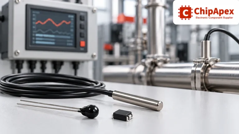
Compare thermistors, RTDs, thermocouples and temperature ICs. Learn how range, accuracy, response, interfaces and mounting affect component selection.
Read More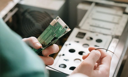
CY7B9910-7SXCT is listed in the Clock Generators, PLLs, Frequency Synthesizers range at ChipApex. The manufacturer field lists Infineon Technologies. Its product description is IC…
Read More
CY7B9910-7SXCT is listed in the Clock Generators, PLLs, Frequency Synthesizers range at ChipApex. The manufacturer field lists Infineon Technologies. Its product description is IC…
Read More
CY7B9910-7SXCT is listed in the Clock Generators, PLLs, Frequency Synthesizers range at ChipApex. The manufacturer field lists Infineon Technologies. Its product description is IC…
Read More
CY7B9910-7SXCT is listed in the Clock Generators, PLLs, Frequency Synthesizers range at ChipApex. The manufacturer field lists Infineon Technologies. Its product description is IC…
Read More
CY7B9910-7SXCT is listed in the Clock Generators, PLLs, Frequency Synthesizers range at ChipApex. The manufacturer field lists Infineon Technologies. Its product description is IC…
Read More
CY7B9910-7SXCT is listed in the Clock Generators, PLLs, Frequency Synthesizers range at ChipApex. The manufacturer field lists Infineon Technologies. Its product description is IC…
Read MoreCY7B9910-7SXCT is listed in the Clock Generators, PLLs, Frequency Synthesizers range at ChipApex. The manufacturer field lists Infineon Technologies. Its product description is IC…
Read More
The activity of extra discounts on wholesale prices is in full swing…
Please fill in your contact information and we will send you the latest wholesale price list.






