ChipApex | Global Electronic Components Supplier

SEARCH
Search Product
Search Post
— IC芯片 | 连接器 | 传感器 | 被动器件 —
Search productSearch post
— IC芯片 | 连接器 | 传感器 | 被动器件 —
Consult the customer manager about the wholesale price.
consultation hotline:86-132-6715-2157
email:[email protected]
Contact the product manager for consultation. One-stop consultation is available.
Do you want a lower wholesale price? Please send us your inquiry and we will reply immediately.
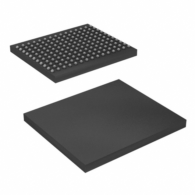
CY7C1263XV18-633BZXC is listed in the Memory IC range at ChipApex. The manufacturer field lists Infineon Technologies. Its product description is IC SRAM 36MBIT PAR 165FBGA. Review the specifications below when checking this part for your BOM.
The CY7C1263XV18-633BZXC is a 36-Mbit QDR II+ Xtreme Synchronous SRAM organized as 2 M x 18. It supports a maximum clock frequency of 633 MHz with double data rate interfaces on both read and write ports, transferring data at 1266 MHz. The device features a four-word burst architecture with 2.5 cycle read latency when the DOFF pin is asserted HIGH. It operates with a core voltage of 1.8 V ± 0.1 V and an I/O voltage range of 1.4 V to 1.6 V. The component is housed in a 165-ball FBGA package.
Verify the specific suffix BZXC against the official Infineon ordering guide to confirm package type and lead-free status. Confirm that the DOFF pin configuration matches the required latency mode, as this affects timing characteristics. Ensure the design accounts for the specified I/O voltage range of 1.4 V to 1.6 V for proper HSTL interface operation.
Select this component for applications requiring high throughput with independent read/write ports. The 633 MHz speed grade offers maximum bandwidth within the QDR II+ Xtreme family. Consider the 2.5 cycle latency requirement and the need for external impedance matching resistors connected to the ZQ pin during system design.
This part belongs to the QDR II+ Xtreme SRAM family developed by Cypress Semiconductor, now part of Infineon Technologies. It shares the same physical footprint and basic interface logic as the CY7C1265XV18, which offers a 1 M x 36 organization. Both devices utilize the same 165-ball FBGA package and support depth expansion through port select inputs.
The CY7C1265XV18 is a compatible alternative within the same family, offering a 1 M x 36 organization instead of 2 M x 18. Verify that the wider data width aligns with the system bus requirements before substitution.
When the DOFF pin is asserted HIGH, the device operates with a 2.5 cycle read latency. If DOFF is asserted LOW or connected to VSS, the device behaves in QDR I mode with a one-cycle read latency.
The ZQ pin is used for impedance matching. An external resistor must be connected between ZQ and ground to tune the output driver impedance to the system data bus impedance.
Explore related parts through Memory, Integrated Circuits (ICs), all product categories, ChipApex homepage.
 CY7C1263XV18-633BZXC
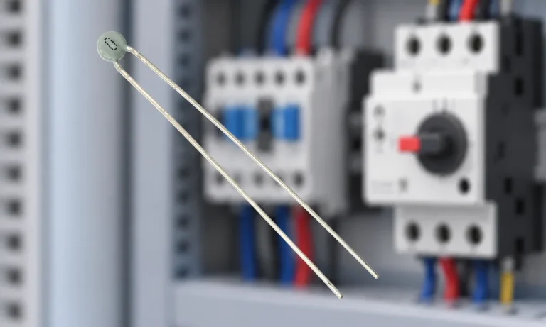
Learn why PTC resistance rises with temperature, how it differs from NTC, and which ratings matter for sensing and protection.
Read More
CY7C1263XV18-633BZXC is listed in the Memory IC range at ChipApex. The manufacturer field lists Infineon Technologies. Its product description is IC SRAM 36MBIT PAR…
Read More
CY7C1263XV18-633BZXC is listed in the Memory IC range at ChipApex. The manufacturer field lists Infineon Technologies. Its product description is IC SRAM 36MBIT PAR…
Read More
CY7C1263XV18-633BZXC is listed in the Memory IC range at ChipApex. The manufacturer field lists Infineon Technologies. Its product description is IC SRAM 36MBIT PAR…
Read More
CY7C1263XV18-633BZXC is listed in the Memory IC range at ChipApex. The manufacturer field lists Infineon Technologies. Its product description is IC SRAM 36MBIT PAR…
Read More
Understand how a comparator switches at a voltage threshold, why hysteresis prevents chatter, and which output and input specs matter.
Read More
See when an inductor behaves linearly, how DC bias and saturation reduce inductance, and which current and temperature curves to check.
Read More
Select power transformers by input frequency, secondary VA, rectifier load, isolation, regulation and inrush. Build a clearer specification for your next RFQ.
Read More
Compare Pt100 and Pt1000 RTDs, two-, three- and four-wire connections, excitation and self-heating. Build an error budget from element to reported temperature.
Read More
Learn what an integrated circuit is, how ICs work, the main types and the specs to check before choosing a part for your design…
Read More
CY7C1263XV18-633BZXC is listed in the Memory IC range at ChipApex. The manufacturer field lists Infineon Technologies. Its product description is IC SRAM 36MBIT PAR…
Read More
CY7C1263XV18-633BZXC is listed in the Memory IC range at ChipApex. The manufacturer field lists Infineon Technologies. Its product description is IC SRAM 36MBIT PAR…
Read More
The activity of extra discounts on wholesale prices is in full swing…
Please fill in your contact information and we will send you the latest wholesale price list.