 ChipApex | Global Electronic Components Supplier

SEARCH
Search Product
Search Post
— IC芯片 | 连接器 | 传感器 | 被动器件 —
Search productSearch post
— IC芯片 | 连接器 | 传感器 | 被动器件 —
Consult the customer manager about the wholesale price.
consultation hotline:86-132-6715-2157
email:[email protected]
Contact the product manager for consultation. One-stop consultation is available.
Do you want a lower wholesale price? Please send us your inquiry and we will reply immediately.
CY7C4251V-15AC is listed in the FIFOs Memory range at ChipApex. The manufacturer field lists Infineon Technologies. Its product description is IC FIFO SYNC 8KX9 11NS 32TQFP. Review the specifications below when checking this part for your BOM.
The CY7C4251V-15AC is a low-voltage synchronous FIFO memory with an 8K x 9 organization, providing 72 kbit of storage. It operates at a maximum frequency of 66.7 MHz with an access time of 11 ns and a cycle time of 15 ns. The device supports a supply voltage range of 3.0 V to 3.6 V and draws a maximum active current of 20 mA in commercial applications. It features independent read and write clocks, programmable Almost Empty/Full flags, and 5V-tolerant inputs. The component is housed in a 32-pin TQFP package.
Verify the specific suffix 'AC' corresponds to the standard 32-lead Thin Quad Flatpack (TQFP) package and Commercial temperature range as defined in the official ordering guide. Confirm that the source documentation explicitly lists this part number variant before procurement, as suffixes dictate package type and operating conditions. Cross-reference the manufacturer's latest selection guide to ensure availability and compliance with current RoHS standards.
Select this component when an 8K depth and 9-bit width are required for synchronous buffering. Ensure the system design accommodates independent Read and Write Clock signals for optimal performance. Verify that the 3.3V supply voltage aligns with the target platform. Consider the 5V-tolerant input feature if interfacing with higher voltage logic levels without additional level shifting circuitry.
This device belongs to the CY7C42X1V family of low-voltage synchronous FIFOs, which includes densities ranging from 64 x 9 to 8K x 9. Manufactured using advanced 0.65 µm P-Well CMOS technology, the family shares common control logic and flag architectures. The CY7C4251V represents the highest density option within this specific series, offering the largest buffer capacity among the listed variants.
CY7C4251V-15AXC
The flags are configured via offset registers accessed through the WEN2/LD pin. When held LOW during reset, this pin enables loading or reading of the empty and full offset values into the internal registers.
If held HIGH at reset, it acts as a second write enable for depth expansion. If held LOW at reset, it functions as a Load (LD) enable to program or read the programmable flag offset registers.
Explore related parts through Logic, Integrated Circuits (ICs), all product categories, ChipApex homepage.
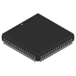 CY7C4251V-15AC
Find out when a bare shock switch needs a pull resistor, when an MCU internal pull-up is enough, and why sensor modules and piezo…
Read More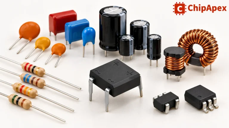
Explore electronic component types, functions, packages and datasheets. Learn selection, replacement and BOM checks before ordering parts for your PCB.
Read More
Compare Hall, shunt, current transformer and Rogowski sensing. Check AC/DC capability, accuracy, isolation, heat and response before selecting a sensor.
Read More
CY7C4251V-15AC is listed in the FIFOs Memory range at ChipApex. The manufacturer field lists Infineon Technologies. Its product description is IC FIFO SYNC 8KX9…
Read More
CY7C4251V-15AC is listed in the FIFOs Memory range at ChipApex. The manufacturer field lists Infineon Technologies. Its product description is IC FIFO SYNC 8KX9…
Read More
CY7C4251V-15AC is listed in the FIFOs Memory range at ChipApex. The manufacturer field lists Infineon Technologies. Its product description is IC FIFO SYNC 8KX9…
Read More
CY7C4251V-15AC is listed in the FIFOs Memory range at ChipApex. The manufacturer field lists Infineon Technologies. Its product description is IC FIFO SYNC 8KX9…
Read More
CY7C4251V-15AC is listed in the FIFOs Memory range at ChipApex. The manufacturer field lists Infineon Technologies. Its product description is IC FIFO SYNC 8KX9…
Read More
CY7C4251V-15AC is listed in the FIFOs Memory range at ChipApex. The manufacturer field lists Infineon Technologies. Its product description is IC FIFO SYNC 8KX9…
Read More
CY7C4251V-15AC is listed in the FIFOs Memory range at ChipApex. The manufacturer field lists Infineon Technologies. Its product description is IC FIFO SYNC 8KX9…
Read More
CY7C4251V-15AC is listed in the FIFOs Memory range at ChipApex. The manufacturer field lists Infineon Technologies. Its product description is IC FIFO SYNC 8KX9…
Read More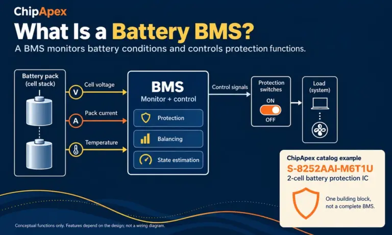
Learn what a battery BMS does, how protection differs from charging, and which pack specifications to check when sourcing BMS components through ChipApex.
Read More
The activity of extra discounts on wholesale prices is in full swing…
Please fill in your contact information and we will send you the latest wholesale price list.





