 ChipApex | Global Electronic Components Supplier
DG409LDY
Search Product
Search Post
— IC芯片 | 连接器 | 传感器 | 被动器件 —
Search productSearch post
— IC芯片 | 连接器 | 传感器 | 被动器件 —
Consult the customer manager about the wholesale price.
consultation hotline:86-132-6715-2157
email:[email protected]
Contact the product manager for consultation. One-stop consultation is available.
Do you want a lower wholesale price? Please send us your inquiry and we will reply immediately.
The DG409LDY is a dual 4-channel differential analog multiplexer manufactured by Vishay Siliconix. It connects one of four differential inputs to a common dual output using a 2-bit binary address (A0, A1). The device operates on single supplies from 3 V to 12 V or dual supplies from ±3 V to ±6 V. Key electrical parameters include a typical drain-source on-resistance of 17 Ω, enable turn-on time of 38 ns, and enable turn-off time of 18 ns. It features low leakage current of 0.2 nA maximum, charge injection of 1 pC, and 82 dB off-isolation at 1 MHz. The component is housed in a 16-pin SOIC package and supports an operating temperature range of -40 °C to +85 °C.
Verify the specific suffix 'LDY' corresponds to the 16-pin narrow SOIC package configuration. Confirm RoHS compliance status if required, as datasheets may list both compliant and non-compliant variants. Ensure the ordering code matches the exact voltage and packaging requirements for the target design.
Select this component when differential signal routing is required within a compact surface-mount footprint. The DG409LDY is suitable for designs needing fast switching speeds and low charge injection. Verify that the supply voltage range aligns with the system's available power rails, as performance varies across different supply configurations.
The DG409LDY belongs to the DG409L series, which serves as a low-voltage companion to the legacy DG409. It utilizes BiCMOS technology to achieve improved performance metrics compared to older CMOS counterparts. This series is designed to maintain pin compatibility while offering enhanced speed and lower power dissipation for modern electronic applications.
DG409LDY-E3
The analog signal range extends from V- to V+, allowing operation across the full supply voltage range of 3 V to 12 V for single supply or ±3 V to ±6 V for dual supply configurations.
It employs a guaranteed break-before-make switching action, which disconnects the previous channel before connecting the new one, thereby protecting against momentary crosstalk between adjacent channels.
The DG409LDY exhibits a typical charge injection of 1 pC, contributing to its high accuracy in precision analog signal processing applications.
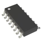 DG409LDY
The activity of extra discounts on wholesale prices is in full swing…
Please fill in your contact information and we will send you the latest wholesale price list.





